6-62 Intel® PXA26x Processor Family Developer’s Manual
Memory Controller
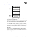
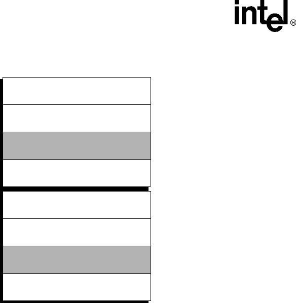
Figure 6-24. 16-Bit PC Card Memory Map
The 16-bit PC Card Memory Map space is divided into eight partitions, four for each card slot. The
four partitions for each card slot are: common memory, I/O, attribute memory, and a reserved
space. Each partition starts on a 64-Mbyte boundary.
During an access, pins MA[25:0], nPREG, and PSKTSEL are driven at the same time. nPCE1 and
nPCE2 are driven concurrently with the address signals for common memory and attribute-
memory accesses. For I/O accesses, their value depends on the value of nIOIS16 and is valid a
fixed amount of time after nIOIS16 is valid.
Common memory and attribute memory accesses assert the nPOE or nPWE control signals. I/O
accesses assert the nIOR or nIOW control signals and use the nIOIS16 input signal to determine
the bus width of the transfer (8 or 16 bits). The PXA26x processor family uses nPCE2 to indicate to
the expansion device that the upper half of the data bus (MD[15:8]) are used for the transfer, and
nPCE1 to indicate that the lower half of the data bus (MD[7:0]) are used. nPCE1 and nPCE2 are
asserted for 16-bit accesses.
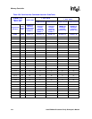
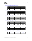
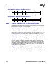
Refer to Table 6-32 through Table 6-39 for signal combinations during common memory, I/O, and
attribute accesses.
When writes goes to a card sockets and a byte has been masked via an internal byte enable, the
write does not occur on the external bus. For reads, one half-word is always read from the socket,
even if only 1 byte is requested. In some cases, based on internal address alignment, one word is
read, even if only 1 byte is requested.
All DMA modes are supported in the card interface increment the address.
Socket 1 Common Memory Space
Socket 1 Attribute Memory Space
Socket 1 I/O Space
Socket 0 Common Memory Space
Socket 0 Attribute Memory Space
Socket 0 I/O Space
Reserved
Reserved
0x3C00 0000
0x3800 0000
0x3400 0000
0x3000 0000
0x2C00 0000
0x2800 0000
0x2400 0000
0x2000 0000


