Intel® PXA26x Processor Family Developer’s Manual 6-3
Memory Controller
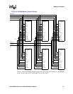
partition pairs: the 0/1 pair and the 2/3 pair. The partitions in a pair must be identical in size and
configuration. The two pairs may be different (for example, the 0/1 pair can be 100-MHz SDRAM
on a 32-bit data bus, while the 2/3 pair can be 50-MHz SDRAM on a 16-bit data bus).
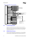
The processor SDRAM Controller includes these signals:
• 4 partition selects (nSDCS[3:0])
• 4 byte selects (DQM[3:0]).
• 15 multiplexed bank/row/column address signals (MA[24:10])
• 1 write enable (nWE)
• 1 column-address strobe (nSDCAS)
• 1 row-address strobe (nSDRAS)
• 1 clock enable (SDCKE[1])
• 2 clocks (SDCLK[2:1])
• 32 data (MD[31:0]).
The processor performs auto-refresh (CBR) during normal operation, and supports self-refreshing
SDRAM during sleep mode. An SDRAM auto-power-down mode bit can be set so that the clock
and clock enable to SDRAM are automatically de-asserted whenever none of the corresponding
partitions is being accessed.
The processor supports x16 and x32 SDRAM chips.
Upon enabling an SDRAM partition, a mode register set command (MRS), is sent to the SDRAM
devices by writing to the MDMRS register. The PXA26x processor family adds support for low-
power SDRAM by giving software access to the Extended Mode Register via the MDMRSLP
register.
MRS commands always configure SDRAM internal mode registers for sequential burst type and a
burst length of four.
The CAS latency is determined by the DTC0 or DTC2 field of MDCNFG.
6.2.2 Static Memory Interface / Variable Latency I/O Interface
The static memory and variable latency I/O (VLIO) interface has six chip selects (nCS[5:0]) and 26
bits of byte address (MA[25:0]) for accesses of up to 64 Mbytes of memory in each of six banks.
Each chip select is individually programmed for selecting one of the supported static memory
types:
• Non-burst ROM or flash memory is supported on nCS[5:0]
• Burst ROM or flash (with non-burst writes) is supported on nCS[5:0] – This is referred to as
page mode in flash documentation
• Burst and non-burst SRAM is supported on nCS[5:0]
• Variable latency I/O is supported on nCS[5:0]
• Synchronous static memory is supported on nCS[3:0] – This is referred to as burst mode in
flash documentation


