


6-30 Intel® PXA26x Processor Family Developer’s Manual
Memory Controller
6.7 Synchronous Static Memory Interface
The synchronous static memory interface supports SMROM and non-SDRAM-like flash
memories. The synchronous static memory can be configured for any of the nCS[3:0] signals. Chip
Select 0 must be used for boot memory. Synchronous static memories in bank pairs 1/0 or 3/2 must
be set to the same timing.
If any of the nCS[3:0] banks are configured for Synchronous Static Memory via
SXCNFG[SXENx], the corresponding half-words of MSC0 (see Section 6.8.2, “Asynchronous
Static Memory Control Registers (MSC0 – 2)”) and MSC1, except the data width in
MSCx[RBWx], are ignored.
6.7.1 Synchronous Static Memory Configuration Register
All synchronous static memory is controlled by the read/write SXCNFG register. Refer to
Table 6-14. SXCNFG[15:0] configures chip select signals 0 and 1. SXCNFG[31:16] configures
chip select signals 2 and 3.
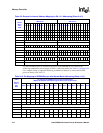
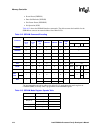
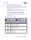
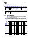
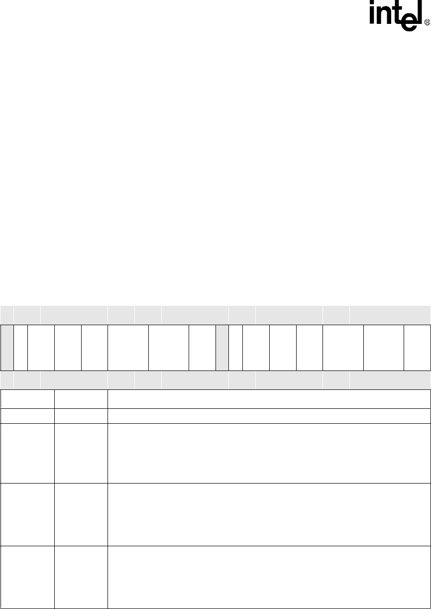
Table 6-14. SXCNFG Register Bitmap (Sheet 1 of 6)
4800 001C SXCNFG
Bit
31 30 29 28 27 26 25 24 23 22 21 20 19 18 17 16 15 14 13 12 11 10 9 8 7 6 5 4 3 2 1 0
Reserved
SXLATCH2
SXTP2
SXCA2
SXRA2
SXRL2
SXCL2
SXEN2
Reserved
SXLATCH0
SXTP0
SXCA0
SXRA0
SXRL0
SXCL0
SXEN0
Reset 0 0 0 0 0 0 0 0 0 0 0 0 0 0 0 0 0 * * * * * * * * * * * * * 0 *
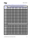
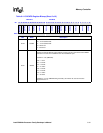
Bits Name Description
31 — Reserved
30 SXLATCH2
SXMEM LATCHING SCHEME FOR PAIR 2/3:
0 – Latch return data with fixed delay on MEMCLK
1 – Latch return data with return clock
Must be set to a 1 to enable the return clock SDCLK for latching data. For more details on
this return data latching.
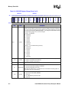
29:28 SXTP2
SX MEMORY TYPE FOR PARTITION PAIR 2/3:
00 – Synchronous Mask ROM (SMROM)
01 – Reserved
10 – Non-SDRAM-like synchronous flash
11 – Reserved
27:26 SXCA2
SX MEMORY COLUMN ADDRESS BIT COUNT FOR PARTITION PAIR 2/3:
00 – 7 column address bits
01 – 8 column address bits
10 – 9 column address bits
11 – 10 column address bits