


4-8 Intel® PXA26x Processor Family Developer’s Manual
System Integration Unit
Note: GPLR2[31:26], GPSR2[31:26], GPCR2[31:26], GPDR2[31:26], GRER2[31:26], GFER2[31:26],
GEDR2[31:26] and GAFR2_U[31:21] are reserved bits. Write zeros to these bits and ignore all
reads from these bits.
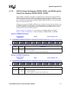
4.1.3.1 GPIO Pin-Level Registers (GPLR0, GPLR1, GPLR2)
Check the state of each of the GPIO pins by reading the GPIO Pin Level Register (GPLR). Each bit
in the GPLR corresponds to one pin in the GPIO. GPLR0[31:0] correspond to GPIO[31:0],
GPLR1[31:0] correspond to GPIO[63:32] and GPLR2[25:0] correspond to GPIO[89:64]. Use the
GPLR0
–2 read-only registers to determine the current value of a particular pin (regardless of the
programmed pin direction). For reserved bits (GPLR2[31:26]), reads return zero.
Table 4-3, Table 4-4, and Table 4-5 show the bitmaps of GPLR0, GPLR1, GPLR2
.
This is a read-only register.
This is read/write register. Ignore reads from reserved bits. Write zeros to reserved bits.
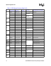
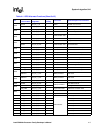
GEDR Detect Edge Type GEDR0 GEDR1 GEDR2
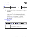
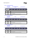
GAFR Set Alternate Functions GAFR0_L GAFR0_U GAFR1_L GAFR1_U GAFR2_L GAFR2_U
NOTE: For the alternate function registers, the designator _L signifies that the lower 16 GPIOs’ alternate functions are configured
by that register and _U designates that the upper 16 GPIOs’ alternate functions are configured by that register.
Table 4-2. GPIO Register Definitions (Sheet 2 of 2)
Register
Type
Register Function GPIO[15:0] GPIO[31:16] GPIO[47:32] GPIO[63:48] GPIO[79:64] GPIO[80]
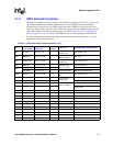
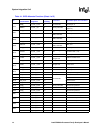
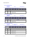
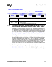
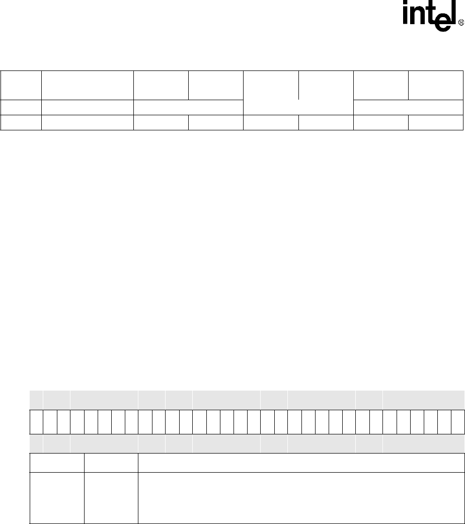
Table 4-3. GPLR0 Bit Definitions
Physical Address
0x40E0_0000
GPLR0 System Integration Unit
Bit
31 30 29 28 27 26 25 24 23 22 21 20 19 18 17 16 15 14 13 12 11 10 9 8 7 6 5 4 3 2 1 0
PL31
PL30
PL29
PL28
PL27
PL26
PL25
PL24
PL23
PL22
PL21
PL20
PL19
PL18
PL17
PL16
PL15
PL14
PL13
PL12
PL11
PL10
PL9
PL8
PL7
PL6
PL5
PL4
PL3
PL2
PL1
PL0
Reset 0 0 0 0 0 0 0 0 0 0 0 0 0 0 0 0 0 0 0 0 0 0 0 0 0 0 0 0 0 0 0 0
Bits Name Description
<31:0> PL[x]
GPIO Pin Level ‘x’ (where x = 0 to 31).
This read-only field indicates the current value of each GPIO.
0 – Pin state is low
1 – Pin state is high