


Intel® PXA26x Processor Family Developer’s Manual 10-17
Universal Asynchronous Receiver/Transmitter
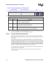
10.4.2.9 Modem Control Register (MCR)
The MCR uses the modem control pins nRTS and nDTR to control the interface with a modem or
data set. The MCR also controls the Loopback mode. Loopback mode must be enabled before the
UART is enabled. The differences between UARTs specific to this register are described in
Section 10.5.1, “UART Register Differences” on page 10-27.
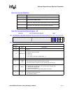
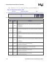
3FE
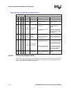
FRAMING ERROR:
Indicates that the received character did not have a valid stop bit. FE is set when the bit
following the last data bit or parity bit is detected to be 0. If the LCR had been set for two
stop bit mode, the receiver does not check for a valid second stop bit. The FE indicator is
reset when the processor reads the LSR. The UART will resynchronize after a framing
error. To do this it assumes that the framing error was due to the next start bit, so it samples
this “start” bit twice and then reads in the “data”. In FIFO mode, FE shows a framing error
for the character at the front of the FIFO, not for the most recently received character.
0 – No Framing error
1 – Invalid stop bit has been detected
2PE
PARITY ERROR:
Indicates that the received data character does not have the correct even or odd parity, as
selected by the even parity select bit. PE is set upon detection of a parity error and is
cleared when the processor reads the LSR. In FIFO mode, PE shows a parity error for the
character at the front of the FIFO, not the most recently received character.
0 – No Parity error
1 – Parity error has occurred
1OE
OVERRUN ERROR:
In non-FIFO mode, indicates that data in the Receive Buffer Register was not read by the
processor before the next character was received. The new character is lost. In FIFO
mode, OE indicates that all 64 bytes of the FIFO are full and the most recently received
byte has been discarded. The OE indicator is set upon detection of an overrun condition
and cleared when the processor reads the LSR.
0 – No data has been lost
1 – Received data has been lost
0DR
DATA READY:
Set when a complete incoming character has been received and transferred into the
Receive Buffer Register or the FIFO. In non-FIFO mode, DR is cleared when the receive
buffer is read. In FIFO mode, DR is cleared if the FIFO is empty (last character has been
read from RBR) or the FIFO is reset with FCR[RESETRF].
0 – No data has been received
1 – Data is available in RBR or the FIFO
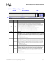
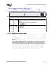
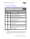
Table 10-13. Line Status Register – LSR (Sheet 2 of 2)
Base+0x14 Line Status Register UART
Bit
31 30 29 28 27 26 25 24 23 22 21 20 19 18 17 16 15 14 13 12 11 10 9 8 7 6 5 4 3 2 1 0
Reserved
FIFOE
TEMT
TDRQ
BI
FE
PE
OE
DR
Reset 0 0 0 0 0 0 0 0 0 0 0 0 0 0 0 0 0 0 0 0 0 0 0 0 0 1 1 0 0 0 0 0
Read only
Bits Name Description