


10-6 Intel® PXA26x Processor Family Developer’s Manual
Universal Asynchronous Receiver/Transmitter
.
10.4.2.1 Receive Buffer Register (RBR)
In non-FIFO mode, the Receive Buffer Register (RBR) holds the character received by the UART’s
Receive Shift Register. If the RBR is configured to use fewer than eight bits, the bits are right-
justified and the most significant bits (MSB) are zeroed. Reading the register empties the register
and clears the Data Ready (DR) bit in the Line Status Register (LSR) to a 0.
In FIFO mode, the RBR latches the value of the data byte at the front of the FIFO.
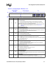
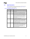
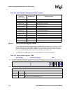
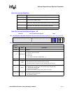
Table 10-2. UART Register Addresses as Offsets of a Base
UART Register
Addresses
(Base + offset)
DLAB Bit Value Register Accessed
Base 0 Receive Buffer (read only)
Base 0 Transmit Buffer (write only)
Base + 0x04 0 Interrupt Enable (read/write)
Base + 0x08 X Interrupt Identification (read only)
Base + 0x08 X FIFO Control (write only)
Base + 0x0C X Line Control (read/write)
Base + 0x10 X Modem Control (read/write)
Base + 0x14 X Line Status (read only)
Base + 0x18 X Modem Status (read only)
Base + 0x1C X Scratch Pad (read/write)
Base + 0x20 X Infrared Selection (read/write)
Base 1 Divisor Latch Low (read/write)
Base + 0x04 1 Divisor Latch High (read/write)
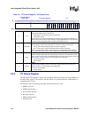
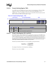
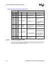
Table 10-3. Receive Buffer Register – RBR
Base (DLAB=0) Receive Buffer Register UART
Bit
31 30 29 28 27 26 25 24 23 22 21 20 19 18 17 16 15 14 13 12 11 10 9 8 7 6 5 4 3 2 1 0
Reserved
RBR7
RBR6
RBR5
RBR4
RBR3
RBR2
RBR1
RBR0
Reset 0 0 0 0 0 0 0 0 0 0 0 0 0 0 0 0 0 0 0 0 0 0 0 0 0 0 0 0 0 0 0 0
Read only
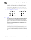
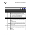
Bits Name Description
[31:8] — Reserved
[7:0] RBR[7:0]
RECEIVE BUFFER REGISTER BITS 7 – 0:
Data byte received least significant bit first.