


11-12 Intel® PXA26x Processor Family Developer’s Manual
Fast Infrared Communication Port
11.3.4 FICP Data Register
The FICP data register (ICDR) is a 32-bit register and its lower 8 bits are the top entry of the
transmit FIFO when the register is written and the bottom entry of the receive FIFO when the
register is read.
Reads to ICDR access the lower 8 bits of the receive FIFO’s bottom entry. As data enters the top of
the receive FIFO, bits 8 – 10 are used as tags to indicate conditions that occur as each piece of data
is received. The tag bits are transferred down the FIFO with the data byte that encountered the
condition. When data reaches the bottom of the FIFO, bit 8 of the FIFO entry is transferred to the
end-of-frame (EOF) flag, bit 9 to the CRC error (CRE) flag, and bit 10 to the receiver overrun
(ROR) flag. All these flags are in FICP status register 1. These flags can be read to determine
whether the value at the bottom of the FIFO represents the frame’s last byte or an error that was
encountered during reception. After the flags are checked, the FIFO value can be read. This causes
the data in the next location of the receive FIFO to be transferred to the bottom entry and its EOF,
CRE, and ROR bits to be transferred to the status register.
The end/error in FIFO (EIF) flag is set in status register 0 when a tag bit is set in any of the receive
FIFO’s bottom eight, 16, or 32 entries, as determined by the trigger level. The EIF flag is cleared
when no error bits are set in the FIFO’s bottom entries. When EIF is set, an interrupt is generated
and the receive FIFO DMA request is disabled. Software must empty the FIFO and check for the
EOF, CRE, and ROR error flags in ICSR1 before it removes each data value from the FIFO. After
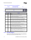
3RXP
RECEIVE PIN POLARITY SELECT.:
0 – Data from the receive data pin is inverted before being used by the FICP unit.
1 – Data from the receive data pin to the FICP unit is not inverted.
Set on reset.
2TXP
TRANSMIT PIN POLARITY SELECT:
0 – Data from the FICP is inverted before being sent to the transmit data pin.
1 – Data from the FICP is not inverted before being sent to the transmit data pin.
Set on reset.
[1:0] TRIG
RECEIVE FIFO TRIGGER LEVEL:
The receive FIFO generates service requests when the FIFO has reached the trigger level
and has no errors in its data. The DMA controller data transfer size must be set to the same
size as the receive FIFO trigger level. To change the trigger level, the receive FIFO must be
disabled.
0b00 – receive FIFO service request is generated when the FIFO has 8 bytes or more
0b01 – receive FIFO service request is generated when the FIFO has 16 bytes or more
0b10 – receive FIFO service request is generated when the FIFO has 32 bytes or more
0b11 – reserved
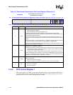
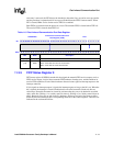
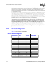
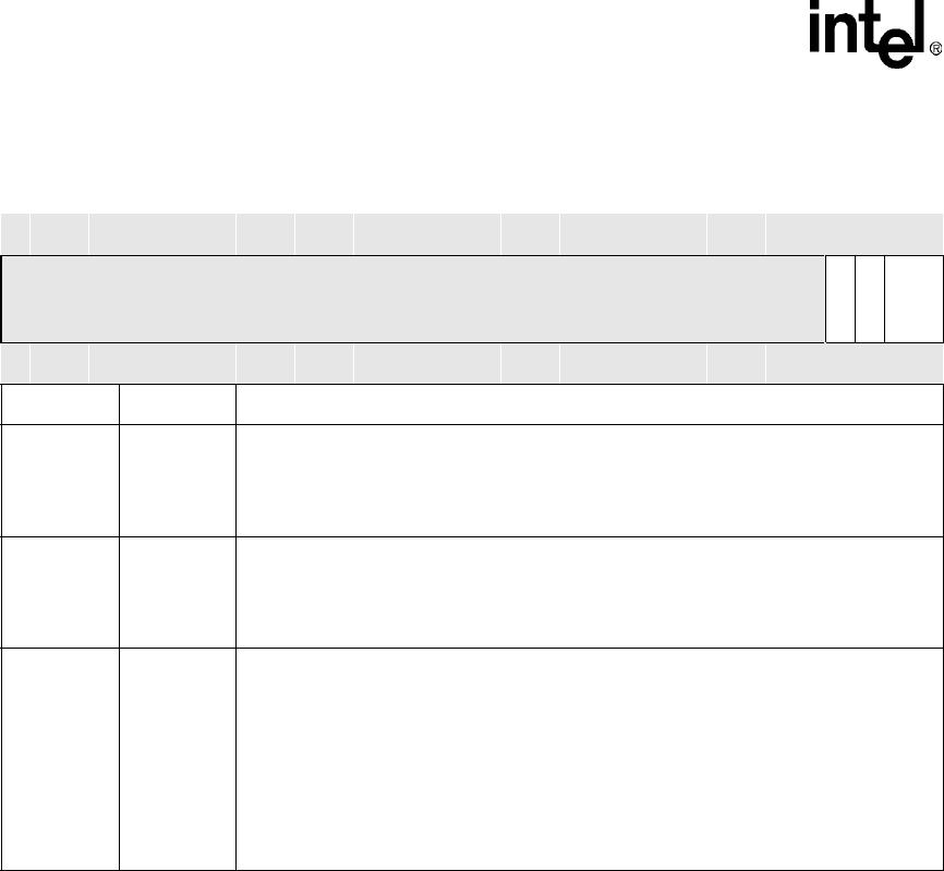
Table 11-4. Fast Infrared Communication Port Control Register 2 (Sheet 2 of 2)
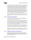
0x4080 0008
Fast Infrared Communication Port
Control Register 2 (ICCR2)
FICP
Bit
31 30 29 28 27 26 25 24 23 22 21 20 19 18 17 16 15 14 13 12 11 10 9 8 7 6 5 4 3 2 1 0
Reserved
RXP
TXP
TRIG
Reset 0 0 0 0 0 0 0 0 0 0 0 0 0 0 0 0 0 0 0 0 0 0 0 0 0 0 0 0 1 1 0 0
Bits Name Description