Intel® PXA26x Processor Family Developer’s Manual 6-13
Memory Controller
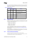
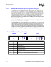
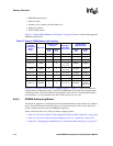
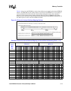
6.6.2.1 Low-Power SDRAM Mode Register Set Configuration Register
Use the Low-Power SDRAM Mode Register Set Configuration register (MDMRSLP) to issue a
special low-power MRS command to SDRAM. Writing this register will trigger a two-stage MRS
command to be issued to external SDRAM. The first stage will write the low- power MRS value to
SDRAM partitions 0 and 1; the second stage will write the low-power MRS value to SDRAM
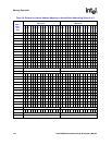
partitions 2 and 3. The value written in this register will be placed directly on address lines
MA[24:10] during the MRS command. When setting the values to be written out on the address
lines, they must be written out properly based on the addressing mode which is being used.
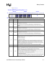
Although writing to this register will trigger an MRS command, the corresponding chip select
values will be asserted only if the memory banks are enabled via the MDCNFG register and if the
corresponding MDMRSLP[MDLPENx] bit is set. To write a new low- power MRS value to
SDRAM, first enable the memory via the MDCNFG register, and then write the MDMRSLP
register with the enable bits set.
This register is not used with in the processor except to write the value during the MRS command.
All values in the MDCNFG register must be programmed correctly to ensure proper operation of
the SDRAM. The register is used by a low-power SDRAM to control the Partial Array Self-
Refresh (PASR) and Temperature Compensated Self-Refresh (TCSR) settings.
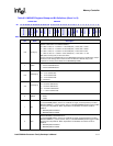
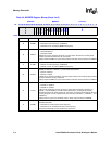
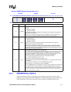
6:4 MDCL0
SDRAM PARTITION PAIR 0 CAS LATENCY – derived from MDCNFG:DTC0. Writes are
ignored. This field is ready-only.
3MDADD0
SDRAM PARTITION PAIR 0 BURST TYPE – Fix to sequential addressing. Writes are
ignored. Always reads 0.
2:0 MDBL0
SDRAM PARTITION PAIR 0 BURST LENGTH – Fixed to a burst length of four. Writes are
ignored. Always reads 010.
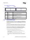
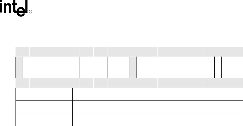
Table 6-4. MDMRS Register Bitmap (Sheet 2 of 2)
0x4800 0040 MDMRS processor
Bit
31 30 29 28 27 26 25 24 23 22 21 20 19 18 17 16 15 14 13 12 11 10 9 8 7 6 5 4 3 2 1 0
Reserved
MDMRS2
MDCL2
MDADD2
MDBL2
Reserved
MDMRS0
MDCL0
MDADD0
MDBL0
Reset 0 0 0 0 0 0 0 0 0 0 1 0 0 0 1 0 0 0 0 0 0 0 0 0 0 0 1 0 0 0 1 0


