


10-8 Intel® PXA26x Processor Family Developer’s Manual
Universal Asynchronous Receiver/Transmitter
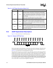
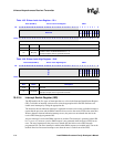
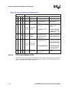
10.4.2.4 Interrupt Enable Register (IER)
The IER enables the five types of interrupts that set a value in the Interrupt Identification Register
(IIR). To disable an interrupt, software must clear the appropriate bit in the IER. Software can
enable some interrupts by setting the appropriate bit.
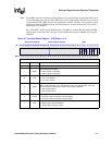
The character timeout indication interrupt is separated from the received data available interrupt to
ensure that the processor and the DMA controller do not service the receive FIFO at the same time.
When a character timeout indication interrupt occurs, the processor must handle the data in the
receive FIFO through programmed I/O.
An error interrupt is used when DMA requests are enabled. The interrupt is generated when LSR
bit 7 is set to a 1, because a receive DMA request is not generated when the receive FIFO has an
error. The error interrupt tells the processor to handle the data in the receive FIFO through
programmed I/O. The error interrupt is enabled when DMA requests are enabled and it can not be
masked. Receiver line status interrupts occur when the error is at the front of the FIFO.
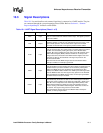
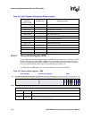
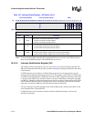
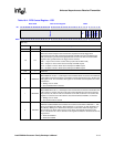
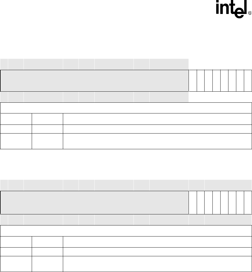
Table 10-5. Divisor Latch Low Register
– DLL
Base (DLAB=1) Divisor Latch Low Register UART
Bit
31 30 29 28 27 26 25 24 23 22 21 20 19 18 17 16 15 14 13 12 11 10 9 876543210
Reserved
DLL7
DLL6
DLL5
DLL4
DLL3
DLL2
DLL1
DLL0
Reset 0 0 0 0 0 0 0 0 0 0 0 0 0 0 0 0 0 0 0 0 0 0 0 000000010
Read/Write
Bits Name Description
31:8 — Reserved
7:0 DLL[7:0]
DIVISOR LATCH LOW REGISTER BITS 7 – 0:
Low byte compare value to generate baud rate.
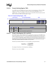
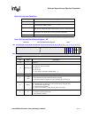
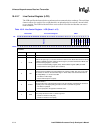
Table 10-6. Divisor Latch High Register – DLH
Base+0x04 (DLAB=1) Divisor Latch High Register UART
Bit
31 30 29 28 27 26 25 24 23 22 21 20 19 18 17 16 15 14 13 12 11 10 9 8 7 6 5 4 3 2 1 0
Reserved
DLH15
DLH14
DLH13
DLH12
DLH11
DLH10
DLH9
DLH8
Reset 0 0 0 0 0 0 0 0 0 0 0 0 0 0 0 0 0 0 0 0 0 0 0 0 0 0 0 0 0 0 0 0
Read/Write
Bits Name Description
31:8 — Reserved
7:0 DLH[15:8]
DIVISOR LATCH HIGH REGISTER BITS 7 – 0:
High byte compare value to generate baud rate.