6-36 Intel® PXA26x Processor Family Developer’s Manual
Memory Controller
6.7.2 Synchronous Static Memory Mode Register Set
Configuration Register
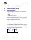
On power up, a MRS command that contains the default boot-up value is written to the external
memory if the system is configured to boot out of SMROM (see Section 6.11.2, “Boot Time
Defaults” on page 6-72). Otherwise, use the Synchronous Static Memory Mode Register Set
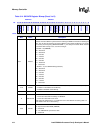
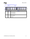
Configuration Register (SXMRS) to issue an MRS command to SMROM. The value written in this
register is placed directly on address lines MA<24:10> during the MRS command. Writing to this
register triggers a two-stage MRS command that is sent to the external synchronous static memory.
The first state issues an MRS command to banks 0 and 1. The second stage issues an MRS
command to banks 2 and 3. The corresponding chip select values are only asserted if the memory
banks are enabled via the SXCNFG register and the memory type is configured as SMROM.
To write a new MRS value to a synchronous static memory, first enable and configure the memory
via the SXCNFG register, then write the SXMRS register. This register is only used for the value
written during the MRS command. All values in the SXCNFG register must be programmed
correctly to ensure proper device operation (refer to the external memory chip product
documentation for proper MRS encoding). Information programmed in the SXCNFG[CL] and
SXCNFG[RL] fields must match any CAS latencies and RAS latencies programmed in this
SXMRS register. Software must ensure that fields match the latencies. In some cases, duplicate
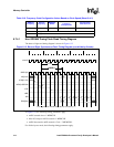
information must be programmed. Refer to Table 6-17.
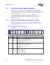
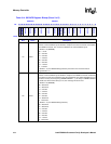
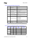
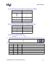
2x13x9x32 2524232221201918171615141312112524 0 1098765432
2x13x9x16 2423222120191817161514131211102423 0 987654321
2x13x10x16 2524232221201918171615141312112524 010987654321
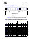
Table 6-16. Synchronous Static Memory External to Internal Address Mapping Options (Sheet
2 of 2)
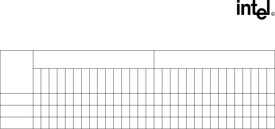
# Bits
Bank x
Row x
Col x
Data
External Address pins at SXMEM RAS Time
MA<24:10>
External Address pins at SXMEM CAS Time
MA<24:10>
24 23 22 21 20 19 18 17 16 15 14 13 12 11 10 24 23 22 21 20 19 18 17 16 15 14 13 12 11 10
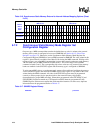
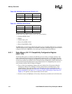
Table 6-17. SXMRS Register Bitmap
4800 0024 SXMRS processor


