


12-26 Intel® PXA26x Processor Family Developer’s Manual
Universal Serial Bus Device Controller
12.6.3 UDC Endpoint x Control/Status Register (UDCCSx), Where
x is 1, 6, or 11
The UDC Endpoint(x) Control Status Register contains 6 bits operate endpoint(x), a bulk IN
endpoint).
12.6.3.1 Transmit FIFO Service (TFS)
The transmit FIFO service bit is active if one or fewer data packets remain in the transmit FIFO.
TFS is cleared when two complete packets of data remain in the FIFO. A complete packet of data is
signified by loading 64 bytes of data or by setting UDCCSx[TSP].
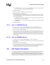
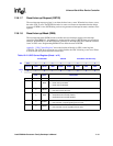
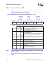
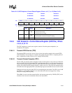
Table 12-13. UDC Endpoint 0 Control Status Register
0h 4060 0010 UDCCS0 Read/Write
Bit
31:8 7 6 5 4 3 2 1 0
Reserved SA RNE FST SST DRWF FTF IPR OPR
Rese
t
X 0 0 0 0 0 0 0 0
Bits Name Description
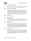
0OPR
OUT PACKET READY (read/write 1 to clear):
1 – OUT packet ready.
1IPR
IN PACKET READY (always read 0/write 1 to set):
1 – IN packet ready.
2FTF
FLUSH Tx FIFO (always read 0/write 1 to set):
1 – Flush the contents of Tx FIFO.
3 DRWF
DEVICE REMOTE WAKE UP FEATURE (read-only):
0 – Device remote wake up feature is disabled.
1 – Device remote wake up feature is enabled.
4SST
SENT STALL (read/write 1 to clear):
1 – UDC sent stall handshake
5FST
FORCE STALL (read/write 1 to set):
1 – Force stall handshake
6RNE
RECEIVE FIFO NOT EMPTY (read-only):
0 – Receive FIFO empty.
1 – Receive FIFO not empty.
7SA
SETUP ACTIVE (read/write 1 to clear):
1 – Setup command is active on the USB
31:8 — Reserved for future use