6-42 Intel® PXA26x Processor Family Developer’s Manual
Memory Controller
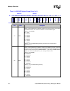
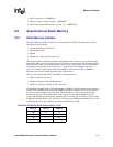
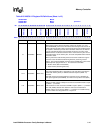
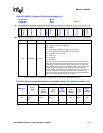
The RT fields in the MSCx registers specify the type of memory:
• Non-burst ROM or flash
• SRAM
• Variable latency I/O
• Burst-of-four ROM or flash
• Burst-of-eight ROM or flash
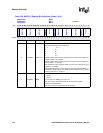
The RBW fields specify the bus width for the memory space selected by nCS[5:0]. For a 16-bit bus
width transactions occur on MD[15:0]. The BOOT_SEL pins or SXCNFG register must be used to
configure nCS[3:0] for SMROM or some other type of Synchronous Static Memory.
6.8.1.1 Static Memory SA-1111 Compatibility Configuration Register
(SA1111CR)
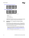
The SA1111CR register was added to the PXA26x processor family to facilitate interfaces that
behave differently based upon the size of the transfer requested, such as a PCI bridge. Normally,
when an 8 or 16 bit read is requested, the PXA26x processor family asserts all DQM signals and
sets the lowest address pins (MA[1:0] for 32 bit external bus and MA[0] for 16 bit external bus) to
zero and discards the unwanted portion of data. When the SA-1111 compatibility bit is set for a
static memory partition, then two things will happen.
• First, on reads for asynchronous memory, the lower address bits will correctly reflect the
starting byte address. This is MA[0] for 16-bit external memory and MA[1:0] for 32-bit
external memory. This is based on the byte enables that may be associated with the read
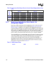
request from the internal bus. See Table 6-22, “32-Bit Byte Address Bits MA[1:0] for Reads
Based on DQM[3:0]” and Table 6-23, “16-Bit Byte Address Bit MA[0] for Reads Based on
DQM[1:0]” for specifics on the external address for this mode.
• Second, on reads, the DQM pins will correctly reflect the byte enables received for the reads.
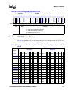
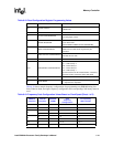
16 bit 00 1100
16 bit 10 0011
32 bit 00 0000
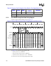
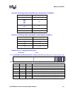
Table 6-21. 16-Bit Bus Write Access
Data Size MA[0] DQM[1:0]
8 bits 0 10
8 bits 1 01
16 bits 0 00
Table 6-20. 32-Bit Bus Write Access (Sheet 2 of 2)
Data Size MA[1:0] DQM[3:0]


