2-20 Intel® PXA26x Processor Family Developer’s Manual
System Architecture
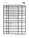
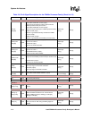
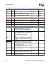
ASSPSFRM/
GPIO[31]
ICOCZ
AUDIO SYNCHRONOUS SERIAL PORT FRAME
SIGNAL
Pulled High
Note [1]
Note [3]
ASSPTXD/
GPIO[30]
ICOCZ AUDIO SYNCHRONOUS SERIAL PORT TRANSMIT
Pulled High
Note [1]
Note [3]
ASSPRXD/
GPIO[29]
ICOCZ AUDIO SYNCHRONOUS SERIAL PORT RECEIVE
Pulled High
Note [1]
Note [3]
HWUART Pins
HWTXD/
GPIO[48]
ICOCZ HARDWARE UART TRANSMIT DATA
Pulled High
Note [1]
Note [3]
HWRXD/
GPIO[49]
ICOCZ HARDWARE UART RECEIVE DATA
Pulled High
Note [1]
Note [3]
HWCTS/
GPIO[50]
ICOCZ HARDWARE UART CLEAR-TO-SEND
Pulled High
Note [1]
Note [3]
HWRTS/
GPIO[51]
ICOCZ HARDWARE UART REQUEST-TO-SEND
Pulled High
Note [1]
Note [3]
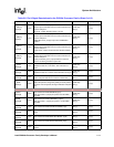
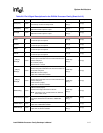
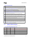
Internal flash pins (See Section 18, “Internal Flash” for more information)
nRST_F IC
RESET FOR FLASH ONLY (input):
Resets internal circuitry and inhibits all operations. Exit
from reset places the flash in asynchronous read-array
mode.
——
nWP_F IC
FLASH WRITE PROTECT (input):
Enables the lock-down mechanism. Blocks locked down
cannot be unlocked with the unlock command. nWP_F
high overrides the lock-down function enabling blocks to
be erased or programmed through software.
——
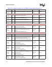
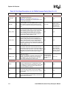
VPEN_F IC
FLASH ERASE/PROGRAM/BLOCK LOCK ENABLE
(input):
Controls device protection. When VPEN_F is less than the
lock voltage, flash contents are protected against Program
and Erase.
——
WAIT_F1
OCZ
FLASH WAIT (output):
Indicates invalid data in synchronous-read (burst) modes.
Not used by the processor, can be used for flash memory
programmers.
——
WAIT_F2
VCC_F SUP
FLASH CORE LOGIC SUPPLY:
Writes to the flash array are inhibited when VCC_F is less
than lockout voltage. Operations at invalid VCC voltages
must not be attempted.
——
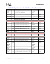
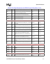
VSS_F SUP
FLASH CORE GROUND:
Ground reference for flash core.
——
VCCQ_F SUP
FLASH I/O POWER SUPPLY:
Must be the same voltage as the PXA26x processor family
VCCN.
——
VSSQ_F SUP
FLASH I/O GROUND:
Ground reference for flash I/O.
——
Table 2-6. Pin & Signal Descriptions for the PXA26x Processor Family (Sheet 12 of 12)
Pin Name Type Signal Descriptions Reset State Sleep State


