


Intel® PXA26x Processor Family Developer’s Manual 7-19
Liquid Crystal Display Controller
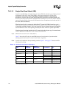
7.6 Liquid Crystal Display Register Descriptions
The LCD controller contains four control registers, ten DMA registers, one status register, and a
256-entry palette RAM. Table 7-16 lists their locations in physical memory. All of the LCD
registers must be accessed as 32-bit values. Reads and writes to undefined addresses in the LCD
register space yield unpredictable results and must not be attempted.
The control registers contain bit fields to:
• Enable and disable the LCD controller
• Define the height and width of the screen being controlled
• Indicate single- or dual-panel display mode
• Indicate color versus monochrome mode
• Indicate passive versus active display
• Set the polarity of the control pins
• Set the pulse width of the line and frame clocks, pixel clock, and ac bias pin frequency
• Set the AC bias pin toggles per interrupt
• Set the number of wait states to insert before and after each line and after each frame
• Enable various interrupt masks
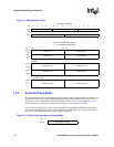
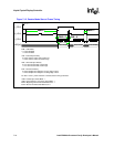
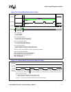
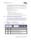
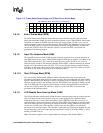
Figure 7-16. Active Mode Pixel Clock and Data Pin Timing
Pixel 0 Pixel 1 Pixel 2 Pixel 3 Pixel 4
PCP - Pixel Clock Polarity
0 - Pixels sampled from data pins on rising edge of clock.
1 - Pixels sampled from data pins on falling edge of clock
.
For PCP = 1 the L_PCLK waveform is inverted, but the timing is identical.
L_FCLK
(
VSYNC)
L_LCLK
(
HSYNC)
L_BIAS
(OE)
L_PCLK
L
DD[15:0]
PCP = 0