


4-18 Intel® PXA26x Processor Family Developer’s Manual
System Integration Unit
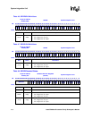
• “00” indicates normal GPIO function for GPIO[85:0]. Indicates default dedicated functionality
for GPIO[89:86].
• “01” selects alternate input function 1 (ALT_FN_1_IN) or alternate output function 1
(ALT_FN_1_OUT) for GPIO[85:0]. Selects GPIO function for GPIO[89:86].
• “10” selects alternate input function 2 (ALT_FN_2_IN) or alternate output function 2
(ALT_FN_2_OUT)
• “11” selects alternate input function 3 (ALT_FN_3_IN) or alternate output function 3
(ALT_FN_3_OUT)
Warning: Configuring a GPIO to map to an alternate function that is not available causes indeterminate
results.
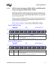
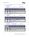
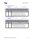
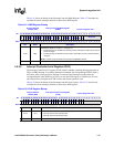
Table 4-24. GAFR0_L Bit Definitions
Physical Address
0x40E0_0054
GAFR0_L System Integration Unit
Bit
31 30 29 28 27 26 25 24 23 22 21 20 19 18 17 16 15 14 13 12 11 10 9 8 7 6 5 4 3 2 1 0
AF15 AF14 AF13 AF12 AF11 AF10 AF9 AF8 AF7 AF6 AF5 AF4 AF3 AF2 AF1 AF0
Reset
0 0 0 0 0 0 0 0 0 0 0 0 0 0 0 0 0 0 0 0 0 0 0 0 0 0 0 0 0 0 0 0
Bits Name Description
<31:0> AF[x]
GPIO PIN ‘X’ ALTERNATE FUNCTION SELECT BITS (where x = 0 through 15):
A bit-pair in this register determines the corresponding GPIO pin’s functionality as one of
the alternate functions that is mapped to it or as a generic GPIO pin.
00 – The corresponding GPIO pin (GPIO[x]) is used as a general purpose I/O.
01 – The corresponding GPIO pin (GPIO[x]) is used for its alternate function 1.
10 – The corresponding GPIO pin (GPIO[x]) is used for its alternate function 2.
11 – The corresponding GPIO pin (GPIO[x]) is used for its alternate function 3.
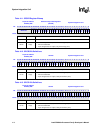
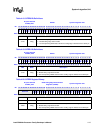
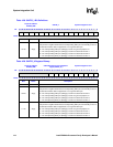
Table 4-25. GAFR0_U Bit Definitions
Physical Address
0x40E0_0058
GAFR0_U System Integration Unit
Bit
31 30 29 28 27 26 25 24 23 22 21 20 19 18 17 16 15 14 13 12 11 10 9 8 7 6 5 4 3 2 1 0
AF31 AF30 AF29 AF28 AF27 AF26 AF25 AF24 AF23 AF22 AF21 AF20 AF19 AF18 AF17 AF16
Reset
0 0 0 0 0 0 0 0 0 0 0 0 0 0 0 0 0 0 0 0 0 0 0 0 0 0 0 0 0 0 0 0
Bits Name Description
<31:0> AF[x]
GPIO PIN ‘X’ ALTERNATE FUNCTION SELECT BITS (where x = 16 through 31):
A bit-pair in this register determines the corresponding GPIO pin’s functionality as one of
the alternate functions that is mapped to it or as a generic GPIO pin.
00 – The corresponding GPIO pin (GPIO[x]) is used as a general purpose I/O.
01 – The corresponding GPIO pin (GPIO[x]) is used for its alternate function 1.
10 – The corresponding GPIO pin (GPIO[x]) is used for its alternate function 2.
11 – The corresponding GPIO pin (GPIO[x]) is used for its alternate function 3.