Intel® PXA26x Processor Family Developer’s Manual 7-37
Liquid Crystal Display Controller
• Number of panels (single or dual)
• Display type (monochrome or color)
• Number of pixel clock wait states programmed at the beginning and end of each line
• Number of line clocks inserted at the beginning and end of each frame
• Width of the VSYNC signal in active mode or VSW line clocks inserted in passive mode
• Width of the frame clock or HSYNC signal.
All of these factors alter the time duration from one frame transmission to the next. Different
display manufacturers require different frame refresh rates, depending on the physical
characteristics of the display. PCD is used to alter the pixel clock frequency in order to meet these
requirements. The frequency of the pixel clock for a set PCD value or the required PCD value to
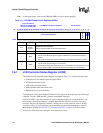
yield a target pixel clock frequency can be calculated using the two following equations. If double
pixel clock mode (DPC) is enabled, PCD must be set greater than or equal to 1.
where:
LCLK = LCD/Memory Clock
PCD = LCCR3[7:0]
7.6.5 LCD Controller DMA
The LCD controller has two fully independent DMA channels that transfer both the palette buffer
and the frame buffer from external memory to the LCD controller. The LCD DMA controller
(DMAC) behaves much like the processor DMAC in descriptor fetch mode. Use DMA channel 0
for single-panel display mode and the upper screen in dual-panel mode. Use DMA channel 1
exclusively for the lower screen in dual-panel mode. Always load the palette RAM through DMA
channel 0. All DMA transfer information is maintained in registers within the LCD DMAC. These
registers are loaded from frame descriptors located in main memory. Use one descriptor per frame
buffer in memory. Use a separate descriptor when the palette RAM is loaded. Multiple descriptors
can be chained together in a list, making it possible for the DMAC to transfer data from an
essentially infinite number of discontiguous locations. The four DMA register types are numbered
according to the associated DMA channel:
• Section 7.6.5.2, “LCD DMA Frame Descriptor Address Registers (FDADRx)”
• Section 7.6.5.3, “LCD DMA Frame Source Address Registers (FSADRx)”
• Section 7.6.5.4, “LCD DMA Frame ID Registers (FIDRx)”
• Section 7.6.5.5, “LCD DMA Command Registers (LDCMDx)”
PixelClock
LCLK
2 PCD 1
+()
--------------------- ---------=
PCD
LCLK
2 PixelClock
()
--------------------- ----------------
1–=


