7-14 Intel® PXA26x Processor Family Developer’s Manual
Liquid Crystal Display Controller
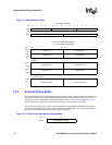
Note: For passive 16 bits per pixel operation, the Raw Pixel Data must be organized as shown above.
)
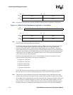
Note: For active 16-bits per pixel operation, the raw pixel data is sent directly to the LCD panel pins and
must be in the format required by the LCD panel.
In dual-panel mode, pixels are presented to two halves of the screen at the same time (upper and
lower). A second DMA channel, input FIFO, and output FIFO exist to support dual-panel
operation. The palette buffer is implemented in DMA channel 0, but not channel 1. The frame-
source address for the lower half always points to the top of the encoded pixel values for channel 1.
The frame-source address of both DMA channels must be configured so the least significant three
address bits are all zero (address bits 2 through 0 must be zero). This requires the frame-buffer-
source address start on 8-byte boundaries.
Each line in the frame buffer must start on a word boundary. For the various pixel sizes, this
requires each line of the display to have pixels in multiples of:
• 32 pixels for 1-bit pixels
• 16 pixels for 2-bit pixels
• 8 pixels for 4-bit pixels
• 4 pixels for 8-bit pixels
• 2 pixels for 16-bit pixels.
If the LCD screen does not naturally have the correct multiple of pixels per line, you must adjust
the start address for each line by adding dummy pixel values to the end of the previous line.
Note: There are two special conditions: 8 bits per pixel monochrome screens with double-pixel-data
mode and 8- or 16-bits per pixel passive color screens require a multiple of 8 pixels for each line.
For example, if the screen being driven is 107-pixels wide, and 4 bits per pixel mode is used, each
line is 107 pixels or nibbles in length (53.5 bytes). The next nearest 8-pixel boundary (for 4-bit
pixels) occurs at 112 pixels or nibbles (56 bytes). Each new line in the frame buffer must start at
multiples of 56 bytes by adding an extra 5-dummy pixels per line (2.5 bytes) to LCCR1[PPL].
Bit 31 16 15 0
Base +
0x0
Pixel 1 Pixel 0
Base +
0x4
Pixel 3 Pixel 2
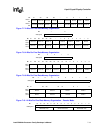
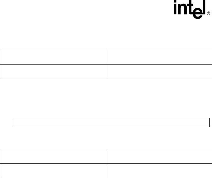
Figure 7-11. 16-Bits Per Pixel Data Memory Organization – Active Mode
Bit 1514131211109876543210
16 bits/pixel Raw Pixel Data<15:0>
Bit 31 16 15 0
Base +
0x0
Pixel 1 Pixel 0
Base +
0x4
Pixel 3 Pixel 2


