


Intel® PXA26x Processor Family Developer’s Manual 4-39
System Integration Unit
4.4.2 Operating System Timer Register Definitions
4.4.2.1 Operating System Timer Match Register 0-3 (OSMR0, OSMR1,
OSMR2, OSMR3)
These registers are 32-bits wide and are readable and writable by the processor. They are compared
against the OSCR after every rising edge of the 3.6864-MHz clock. If any of these registers match
the counter register, and the appropriate interrupt enable bit is set, then the corresponding status bit
in the OSSR is set. The status bits are routed to the interrupt controller where they can be unmasked
to cause a CPU interrupt. You may also use the OSMR3 as a watchdog timer.
Table 4-44 shows the bitmap of the OS Timer Match register. All four registers are identical, except
for location. A single, generic OS Timer match register is described, but all information is common
to all four OS Timer Match Registers.
4.4.2.2 Operating System Timer Interrupt Enable Register (OIER)
This register contains four enable bits that indicate whether a match between one of the match
registers and the OS timer counter sets a status bit in the OSSR. Each match register has a
corresponding enable bit. Clearing an enable bit does not clear the corresponding interrupt status
bit if it is already set.
Table 4-45 shows the bitmap of the OS Timer Interrupt Enable register.
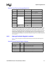
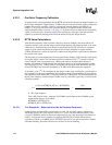
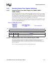
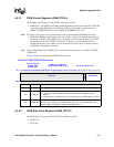
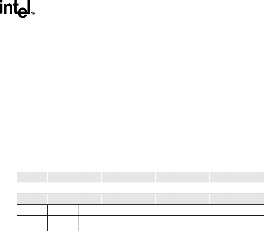
Table 4-44. OSMR[x] Bit Definitions
Physical Address
0x40A0_0000
0x40A0_0004
0x40A0_0008
0x40A0_000C
OS Timer Match Registers
(OSMR3, OSMR2, OSMR1,
OSMR0)
System Integration Unit
Bit
31 30 29 28 27 26 25 24 23 22 21 20 19 18 17 16 15 14 13 12 11 10 9 8 7 6 5 4 3 2 1 0
OSMV
Reset
0 0 0 0 0 0 0 0 0 0 0 0 0 0 0 0 0 0 0 0 0 0 0 0 0 0 0 0 0 0 0 0
Bits Name Description
<31:0> OSMV
OS TIMER MATCH VALUE:
The value compared against the OS timer counter.