Intel® PXA26x Processor Family Developer’s Manual 16-25
Network/Audio Synchronous Serial Protocol Serial Ports
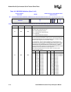
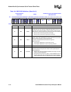
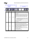
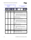
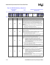
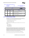
14 R/W EFWR
ENABLE FIFO WRITE/READ (test mode bit):
Enables test mode for the SSP port.
When set, the port enters a mode that whenever the CPU reads or
writes to the SSP Data register, it reads and writes directly to either the
transmit FIFO or the receive FIFO, depending on the programmed state
of STRF.
In EFWR test mode, data is not transmitted on the SSPTXD pin, data
input on the SSPRXD pin is not stored, and the busy and ROR bits have
no effect. However, the Interrupt Test Register is still functional. Using
software, this mode can test whether or not the transmit FIFO or the
receive FIFO operates properly as a FIFO memory stack.
0 – FIFO write/read special function is disabled (normal SSP port
operational mode)
1 – FIFO write/read special function is enabled.
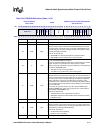
13:10 R/W RFT
RECEIVE FIFO THRESHOLD:
Sets the trigger threshold at which the receive FIFO asserts interrupt.
This level must be set to the desired trigger threshold value minus 1.
This value sets the level at or above which the FIFO controller triggers a
DMA service request (if enabled) or a CPU interrupt request (if
enabled).
9:6 R/W TFT
Transmit FIFO Threshold sets the trigger threshold at which transmit
FIFO asserts interrupt. This level must be set to the desired trigger
threshold value minus 1.
This value sets the level at or below which the FIFO controller triggers a
DMA service request (if enabled) or a CPU interrupt request (if
enabled).
5R/WMWDS
MICROWIRE TRANSMIT DATA SIZE:
Selects between an eight bit or 16-bit size for the command word
transmitted using the Microwire* protocol. MWDS is ignored for all other
frame formats.
0 – 8-bit command words are transmitted.
1 – 16-bit command words are transmitted.
4 R/W SPH
SPI* SSPSCLK PHASE SETTING:
0 – SSPSCLK is inactive one cycle at the start of a frame and 1/2 cycle
at the end of a frame.
1 – SSPSCLK is inactive 1/2 cycle at the start of a frame and one cycle
at the end of a frame.
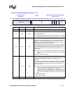
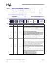
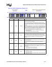
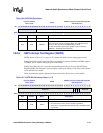
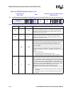
Table 16-4. SSCR1 Bit Definitions (Sheet 5 of 6)
Physical Address
Base+0x04
SSCR1
PXA26x processor family Network/Audio
SSP Serial Ports
Bit
31 30 29 28 27 26 25 24 23 22 21 20 19 18 17 16 15 14 13 12 11 10 9 8 7 6 5 4 3 2 1 0
TTELP
TTE
EBCEI
SCFR
Reserved
SCLKDIR
SFRMDIR
RWOT
Reserved
TSRE
RSRE
TINTE
Reserved
STRF
EFWR
RFT TFT
MWDS
SPH
SPO
LBM
TIE
RIE
Reset 0 0 0 0 ? ? 0 0 0 0 0 0 0 ? ? ? 0 0 0 0 0 0 0 0 0 0 0 0 0 0 0 0
Bits Access Name Description


