


Intel® PXA26x Processor Family Developer’s Manual 9-7
Inter-Integrated Circuit Bus Interface Unit
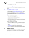
8. Repeated START (Repeat Step 1) or STOP
9.4.1 Serial Clock Line (SCL) Generation
When the I
2
C unit is in master-transmit or master-receive mode, it generates the I
2
C clock output.
The SCL clock is generated by setting the ICR[FM] bit for either 100 KBit/sec or 400 Kbit/sec
operation.
9.4.2 Data and Addressing Management
The I
2
C Data Buffer Register (IDBR) and the I
2
C Slave Address Register (ISAR) manage data and
slave addressing. The IDBR (see Section 9.9.2, “I2C Data Buffer Register- IDBR”) contains one
byte of data or a 7-bit slave address and the R/nW bit. The ISAR contains the processor
programmable slave address. The I
2
C unit puts received data in the IDBR after a full byte is
received and acknowledged. To transmit data, the CPU writes to the IDBR, and the I
2
C unit passes
the information to the serial bus when the ICR[TB] bit is set. See Section 9.9.3, “I2C Control
Register- ICR”.
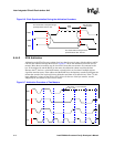
When the I
2
C unit is in master- or slave-transmit mode:
• Software writes data to the IDBR over the internal bus. This initiates a master transaction or
sends the next data byte after the ISR[ITE] bit is set.
• I
2
C unit transmits data from the IDBR when the ICR[TB] bit is set.
• When enabled, an IDBR transmit empty interrupt is signalled when a byte is transferred on the
I
2
C bus and the acknowledge cycle is complete.
• When the I
2
C unit is ready to transfer the next byte before the CPU has written the IDBR and
a STOP condition is not in place, the I
2
C unit inserts wait states until the CPU writes a new
value into the IDBR and sets the ICR[TB] bit.
When the I
2
C unit is in master- or slave-receive mode:
• The processor reads IDBR data over the internal bus after the IDBR receive full interrupt is
signalled.
• I
2
C unit transfers data from the shift register to the IDBR after the acknowledge cycle
completes.
• I
2
C unit inserts wait states until the IDBR is read. Refer to Section 9.4.3, “Inter-Integrated
Circuit Acknowledge” for acknowledge pulse information in receiver mode.
• After the CPU reads the IDBR, the I
2
C unit writes the ICR[ACKNAK] bit and the ICR[TB]
bit, allowing the next byte transfer to proceed.
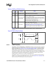
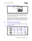
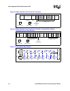
9.4.2.1 Addressing a Slave Device
As a master device, the I
2
C unit must compose and send the first byte of a transaction. This byte
consists of the slave address for the intended device and a R/nW bit for transaction definition. The
MSB is transmitted first. The slave address and the R/nW bit are written to the IDBR (see
Figure 9-4 on page 9-8).