


Intel® PXA26x Processor Family Developer’s Manual 7-33
Liquid Crystal Display Controller
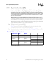
7.6.3.4 Lines Per Panel (LPP)
The lines per panel (LPP) bit field specifies the number of lines or rows present on the LCD panel
being controlled. In single-panel mode, it represents the total number of lines for the entire LCD
display. LPP is used to count the correct number of line clocks that must occur before the frame
clock can be pulsed. In dual-panel mode, it represents half the number of lines of the entire LCD
display, which is split into two panels. LPP is a 10-bit value that represents between 1 and 1024
lines per screen. It must be programmed with the actual height of the display minus one. It is
recommended not to exceed 480 pixels. For portrait mode panels, more than 480 pixels can be used
as long as total pixels do not exceed 307,200. For example, a 480x640 portrait mode panel can be
used.
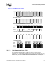
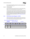
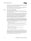
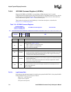
7.6.4 LCD Controller Control Register 3 (LCCR3)
LCD Controller Control Register 3, shown in Table 7-6, contains bits and bit fields that control
various functions within the LCD controller. This register is read/write. Reserved bits must be
written with zeros and reads from them must be ignored.
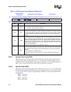
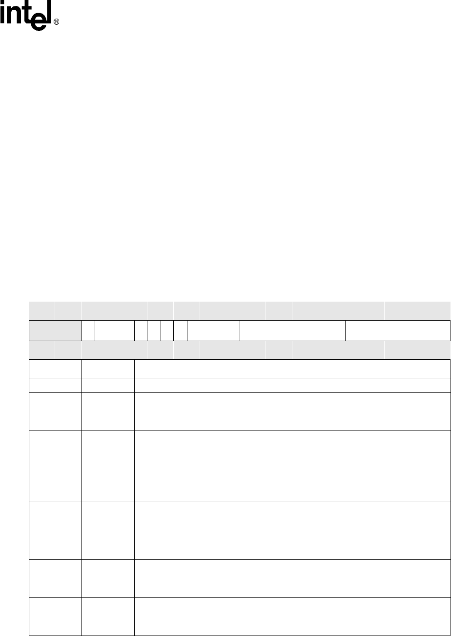
Table 7-6. LCD Controller Control Register 3 (Sheet 1 of 2)
Physical Address
0x4400_000C
LCD Controller Control Register 3 LCD Controller
Bit
31 30 29 28 27 26 25 24 23 22 21 20 19 18 17 16 15 14 13 12 11 10 9 8 7 6 5 4 3 2 1 0
reserved
DPC
BPP
OEP
PCP
HSP
VSP
API ACB PCD
Reset
X X X X 0 0 0 0 0 0 0 0 0 0 0 0 0 0 0 0 0 0 0 0 0 0 0 0 0 0 0 0
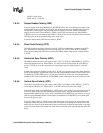
Bits Name Description
31:28 — Reserved – Write with zeros.
27 DPC
DOUBLE PIXEL CLOCK MODE (Section 7.6.4.1):
0 – The L_PCLK pin is driven at the frequency specified by PCD.
1 – The L_PCLK pin is driven at double the frequency specified by PCD.
26:24 BPP
BITS PER PIXEL (Section 7.6.4.2):
000 – 1-bits/pixel [4 entry, 8 byte palette buffer (only first 2 entries are used)]
001 – 2-bits/pixel [4 entry, 8 byte palette buffer]
010 – 4-bits/pixel [16 entry, 32 byte palette buffer]
011 – 8-bits/pixel [256 entry, 512 byte palette buffer]
100 – 16-bits/pixel [no palette buffer]
101, 110, 111 – reserved
23 OEP
OUTPUT ENABLE POLARITY (Section 7.6.4.3):
0 – L_BIAS pin is active high and inactive low in active display mode.
1 – L_BIAS pin is active low and inactive high in active display mode.
In active display mode, data is driven out to the LCD’s data pins on the programmed pixel
clock edge when the L_BIAS pin is active. OEP is ignored in passive display mode.
22 PCP
PIXEL CLOCK POLARITY (Section 7.6.4.4):
0 – Data is sampled on the LCD data pins on the rising edge of L_PCLK.
1 – Data is sampled on the LCD data pins on the falling edge of L_PCLK.
21 HSP
HORIZONTAL SYNC POLARITY (Section 7.6.4.5):
0 – L_LCLK pin is active high and inactive low.
1 – 1 – L_LCLK pin is active low and inactive high.