Intel® PXA26x Processor Family Developer’s Manual 7-23
Liquid Crystal Display Controller
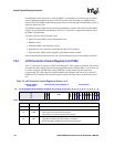
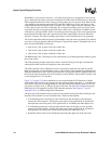
After a word of palette data is written to the input FIFO, the value contained within PDD is loaded
to a down counter. The down counter disables the palette from issuing another DMA request until
the counter decrements to zero. This counter ensures that the LCD’s DMAC does not tie up the full
bandwidth of the processor system bus. Once the counter reaches zero, any pending or future DMA
requests by the palette cause the DMAC to arbitrate for the bus. Once the DMA burst cycle has
completed, the process starts over, and the value in PDD is loaded to the counter to create another
wait state period, which disables the palette from issuing a DMA request. PDD can be programmed
with a value that causes the FIFO to wait from 0 to 255-clock cycles after the completion of one
DMA request to the start of the next request. When PDD=0x00, the FIFO DMA request delay
function is disabled.
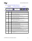
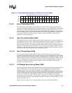
7.6.1.4 LCD Quick Disable Interrupt Mask (QDM)
The LCD quick disable interrupt mask (QDM) bit masks interrupt requests that are asserted after
the LCD enable bit (ENB) is cleared and the DMAC finishes the current burst transfer. The LCD
controller immediately stops requesting new data and the current frame is not completed. This
shutdown is for sleep shutdown. When QDM=0, the quick disable interrupt is enabled, and
whenever the LCSR[QD] status bit is set, an interrupt request is made to the interrupt controller.
When QDM=1, the quick disable interrupt is masked and the state of the QD status bit is ignored
by the interrupt controller. Setting QDM does not affect the current state of QD or the LCD
controller’s ability to set and clear QD, it only blocks the generation of the interrupt request.
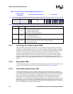
7.6.1.5 LCD Disable (DIS)
During LCD controller operation, setting DIS=1 causes the LCD controller to finish fetching the
current frame from memory and then cleanly shuts down. If the LCD DMAC is loading the palette
RAM when DIS is set, the load will complete followed by the next frame, and then the LCD
controller is disabled. Completion of the current frame is signalled by the LCD when it sets
LCSR[LDD]. Use a read-modify-write procedure to set this bit, since the other bit fields within
LCCR0 continue to be used until the current frame is completed. The LCD Enable bit (ENB) is
cleared when the disable is completed. Refer to Section 7.2.2, “Disabling the Controller” for more
information.
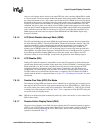
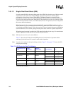
7.6.1.6 Double-Pixel Data (DPD) Pin Mode
The double-pixel data (DPD) pin mode bit selects whether four or eight data pins are used for pixel
data output to the LCD screen in single-panel monochrome mode. When DPD=0, L_DD[3:0] pins
are used to send 4 pixel values each pixel clock transition. When DPD=1, L_DD[7:0] pins are used
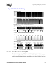
to send 8 pixel values each pixel clock. See Table 7-3 for a comparison of how the LCD’s data pins
are used in each of its display modes.
Note: DPD does not affect dual-panel monochrome mode, any of the color modes, or active mode. Clear
DPD in these modes.
7.6.1.7 Passive/Active Display Select (PAS)
The passive/active display select (PAS) bit selects whether the LCD controller operates in passive
(STN) or active (TFT) display control mode. When PAS=0, passive mode is selected. All LCD data
flow operates normally (including the LCD’s dither logic), and all LCD controller pin timing
operates as described in Table 7.5.


