Intel® PXA26x Processor Family Developer’s Manual 2-19
System Architecture
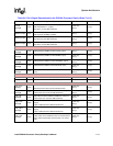
TMS IC
JTAG TEST MODE SELECT (input):
Selects the test mode required from the JTAG controller.
This pin has an internal pull-up resistor.
Input Input
TCK IC
JTAG TEST CLOCK (input):
Clock for all transfers on the JTAG test interface.
Input Input
TEST IC
TEST MODE (input):
Reserved. Must be grounded.
Input Input
TESTCLK IC
TEST CLOCK (input):
Reserved. Must be grounded.
Input Input
Power and Ground Pins
VCC SUP
INTERNAL LOGIC POSITIVE SUPPLY:
Must be connected to the low voltage (.85 – 1.3v) supply
on the PCB.
Powered Note [6]
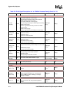
VSS SUP
INTERNAL LOGIC GROUND SUPPLY:
Must be connected to the common ground plane on the
PCB.
Grounded Grounded
PLL_VCC SUP
PLLS AND OSCILLATORS POSITIVE SUPPLY:
Must be connected to the common low voltage supply.
Powered Note [6]
PLL_VSS SUP
PLL GROUND SUPPLY:
Must be connected to common ground plane on the PCB.
Grounded Grounded
VCCQ SUP
CMOS I/O POSITIVE SUPPLY:
EXCEPT memory bus and PCMCIA pins. Must be
connected to the common 2.775 – 3.3v supply on the
PCB.
Powered Note [7]
VSSQ SUP
CMOS I/O GROUND SUPPLY:
Except memory bus and PCMCIA pins. Must be
connected to the common ground plane on the PCB.
Grounded Grounded
VCCN SUP
MEMORY BUS AND PCMCIA PINS POSITIVE SUPPLY:
Must be connected to the common 2.5 – 3.3v supply on
the PCB.
Powered Note [7]
VSSN SUP
MEMORY BUS AND PCMCIA PINS GROUND SUPPLY:
Must be connected to the common ground plane on the
PCB.
Grounded Grounded
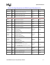
Network SSP pins
NSSPSCLK/
GPIO[81]
ICOCZ NETWORK SYNCHRONOUS SERIAL PORT CLOCK
Pulled High
Note [1]
Note [3]
NSSPSFRM/
GPIO[82]
ICOCZ
NETWORK SYNCHRONOUS SERIAL PORT FRAME
SIGNAL
Pulled High
Note [1]
Note [3]
NSSPTXD/
GPIO[83]
ICOCZ NETWORK SYNCHRONOUS SERIAL PORT TRANSMIT
Pulled High
Note [1]
Note [3]
NSSPRXD/
GPIO[84]
ICOCZ NETWORK SYNCHRONOUS SERIAL PORT RECEIVE
Pulled High
Note [1]
Note [3]
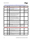
Audio SSP Pins
ASSPSCLK/
GPIO[28]
ICOCZ AUDIO SYNCHRONOUS SERIAL PORT CLOCK
Pulled High
Note [1]
Note [3]
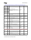
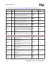
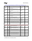
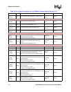
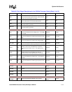
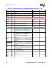
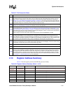
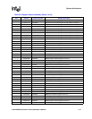
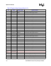
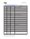
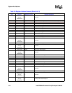
Table 2-6. Pin & Signal Descriptions for the PXA26x Processor Family (Sheet 11 of 12)
Pin Name Type Signal Descriptions Reset State Sleep State


