


7-8 Intel® PXA26x Processor Family Developer’s Manual
Liquid Crystal Display Controller
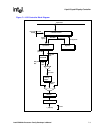
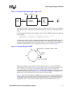
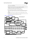
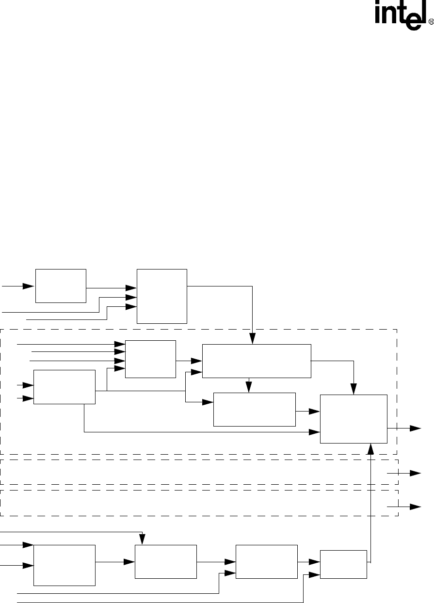
1. The new CV is sent through the color offset adjuster, where it is used as a lookup into the
matrix selected by TCR[COAM].
2. Either the 8-bit output of the chosen matrix or 00h, as selected by TCR[COAE], is added to the
appropriate color’s seed register value in register TRGBR to form an offset.
3. This offset is added to the result of the multiplication of the frame number and the CV to form
the algorithm’s lower boundary (only the lower 8 bits are used).
4. The CV is added to the lower boundary to obtain the upper boundary.
5. Row (line) and column (pixel) counters are combined with beat suppression (offset) values in
the pixel number adjuster and address generator to form yet another address for a matrix
lookup.
6. The output of the chosen matrix is compared to the lower and upper boundaries in the data
generator.
7. If the matrix output is between these boundaries or the original pixel value is 254 or 255, then
the data output to the panel is one. In all other cases, it is zero.
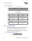
Figure 7-4. TMED Block Diagram
Lower Boundary
LB =FN x CV + Offset
Generator
Frame
Counter
Upper Boundary
UB =LB + CV
Generator
Color Value
Generator
Color
Offset
Adjuster
Data
Generator
LB > ME > UB
or Pixel > 253
Single Color Component Path (GREEN)
Single Color Component Path (BLUE)
Single Color Component Path (RED)
Output
Data
Bit
Frame
Number
Adjuster
FN
CV
LB
UB
LB
Output
Data
Bit
Output
Data
Bit
Line Counter
Pixel Number
Adjustor
Address
Generator
Matrix
Pixel Counter
frame_clk
line clk
pixel clk
TMED Control Register (TCR)
TCR<13:12>
pixel
data
TCR<1>
TCR<0>
TCR<2>
TMED Seed Register (TSR)
TSR<7:0>
TCR<3>
TCR<14>
TCR<11:8>
TCR<7:4>
force to 1
ME