


6-18 Intel® PXA26x Processor Family Developer’s Manual
Memory Controller
• SDRAM timing category
• Data-bus width
• Number of row, column, and bank address bits
• Addressing scheme
• Data-latching scheme
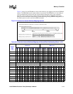
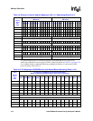
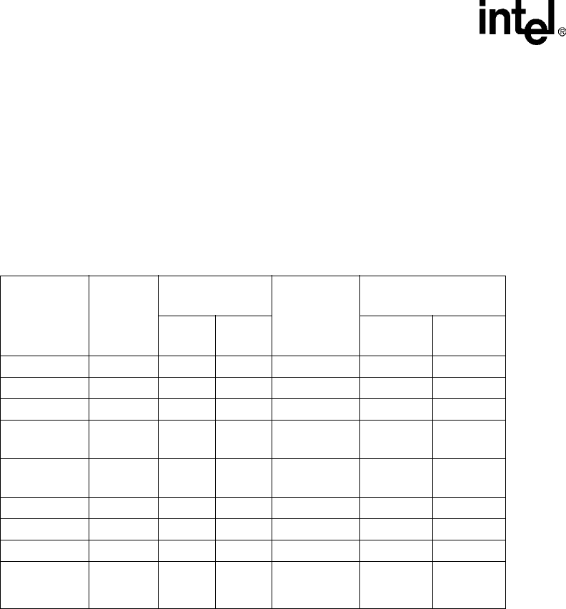
Table 6-7, “Sample SDRAM Memory Size Options” on page 6-18 shows a sample of the supported
SDRAM configurations.
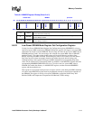
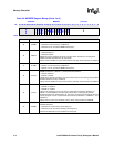
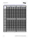
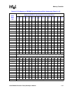
Figure 6-4, “External to Internal Address Mapping Options” on page 6-19 shows the bank/row/
column address multiplexing using a 2x13x9 32-bit SDRAM as an example for the normal bank-
addressing scheme. All unused address bits during RAS and CAS time - including MA[9:0] bits
not shown here - are not guaranteed, and will be either driven to zero or one.
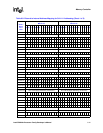
6.6.4.1 SDRAM Addressing Modes
The processor supports two addressing modes: Normal Bank Address mode and SA-1111 Address
mode. The addressing mode alters the order of the address bits that are driven on the individual
memory address pins and control the SDRAM components.
.Refer to the tables below for a listing of address mapping options.
• Table 6-8, “External to Internal Address Mapping for Normal Bank Addressing” on page 6-19
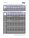
• Table 6-9, “External to Internal Address Mapping for SA-1111 Addressing” on page 6-21.
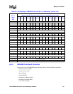
• Table 6-10, “Pin Mapping to SDRAM Devices with Normal Bank Addressing” on page 6-22
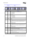
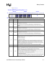
Table 6-7. Sample SDRAM Memory Size Options
SDRAM
Configuration
(Words x
Bits)
Chip Size
Number Chips/
Partition
Bank Bits x
Row Bits x
Column Bits
Partition Size
(Mbyte/Partition)
16-Bit
Bus
32-Bit
bus
16-Bit
Bus
32-Bit
Bus
1M x 16 16 Mbit 1 2 1 x 11 x 8 2 Mbyte 4 Mbyte
2 M x 8 16 Mbit 2 4 1 x 11 x 9 4 Mbyte 8 Mbyte
2 M x 32 64 Mbit N/A 1 2 x 11 x 8 N/A 8 Mbyte
4 M x 16 64 Mbit 1 2
1 x 13 x 8
2 x 12 x 8
8 Mbyte 16 Mbyte
8 M x 8 64 Mbit 2 4
1 x 13 x 9
2 x 12 x 9
16 Mbyte 32 Mbyte
8 M x 16 128 Mbit 1 2 2 x 12 x 9 16 Mbyte 32 Mbyte
16 M x 8 128 Mbit 2 4 2 x 12 x 10 32 Mbyte 64 Mbyte
16 M x 16 256 Mbit 1 2 2 x 13 x 9 32 Mbyte 64 Mbyte
32 M x 8 256 Mbit 2 4 2 x 13 x 10 64 Mbyte
128 Mbyte -
exceeds
partition size