4-48 Intel® PXA26x Processor Family Developer’s Manual
System Integration Unit
The output waveform in Figure 4-4 is created by writing PWM_PERVALn[PV] with a decimal
value of 10 (11 clocks) and PWM_DUTYn[DCYCLE] with 6. Figure 4-4 also shows that
PWM_CTRLn[PRESCALE] is configured with a value of 0x0 loaded, which results in the
PSCLK_PWMn having the same frequency as the 3.6864-MHz-input clock.
4.5.4 Register Summary
Table 4-49 shows the registers associated with the OS timer and the physical addresses used to
access them.
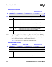
Table 4-53. PWM Register Locations
Address Name Description
0x40B0_0000 PWM_CTRL0 PWM0 Control Register
0x40B0_0004 PWM_PWDUTY0 PWM0 Duty Cycle Register
0x40B0_0008 PWM_PERVAL0 PWM0 Period Control Register
0x40C0_0000 PWM_CTRL1 PWM1 Control Register
0x40C0_0004 PWM_PWDUTY1 PWM1 Duty Cycle Register
0x40C0_0008 PWM_PERVAL1 PWM1 Period Control Register


