16-28 Intel® PXA26x Processor Family Developer’s Manual
Network/Audio Synchronous Serial Protocol Serial Ports
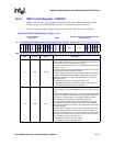
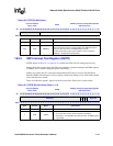
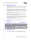
16.5.4 SSP Time Out Register (SSTO)
SSP Time Out Register, shown in Table 16-6,specifies the time-out value used to signal a period of
inactivity within the receive FIFO.
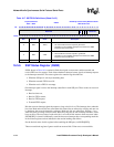
These are read/write registers. Ignore reads from reserved bits. Write zeros to reserved bits.
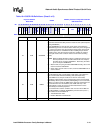
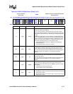
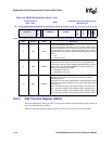
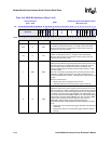
3R/WETDS
END OF TRANSFER DATA STATE:
Determines the state of SSPTXD at the end of a transfer. When cleared,
the state of SSPTXD is forced to 0 after the last bit (bit 0) of the frame is
sent and remains 0 through the next idle period. When set, the state of
SSPTXD retains the value of the last bit sent (bit 0) through the next idle
period.
0 – Low
1 – Last Value <Bit 0>
2R/WSFRMP
SERIAL FRAME POLARITY:
Determines the active state of the Serial Frame signal (SSPSFRM).
In Idle mode or when the SSP is disabled, SSPSFRM is in its inactive
state. In slave mode (SSCR1[SFRMDIR] set), this bit indicates the
polarity of the incoming frame signal.
0 – SSPSFRM is active low.
1 – SSPSFRM is active high.
1:0 R/W SCMODE
SERIAL BIT-RATE CLOCK MODE:
Selects one of four serial clock modes when the PSP is selected
(SSCR0[FRF]=0b11).
Its operation is similar to how SSCR1[SPO] and SSCR1[SPH] together
determine the idle state of SSPSCLK and on which edges data is driven
and sampled.
0b00 - Data Driven (Falling), Data Sampled (Rising), Idle State (Low)
0b01 - Data Driven (Rising), Data Sampled (Falling), Idle State (Low)
0b10 - Data Driven (Rising), Data Sampled (Falling), Idle State (High)
0b11- Data Driven (Falling), Data Sampled (Rising), Idle State (High)
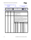
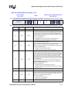
Table 16-5. SSPSP Bit Definitions (Sheet 2 of 2)
Physical Address
Base + 0x2C
SSPSP
PXA26x processor family Network/Audio
SSP Serial Ports
Bit
31 30 29 28 27 26 25 24 23 22 21 20 19 18 17 16 15 14 13 12 11 10 9 8 7 6 5 4 3 2 1 0
Reserved
DMYSTOP
Reserved
SFRMWDTH SFRMDLY
DMYSTRT
STRTDLY
ETDS
SFRMP
SCMODE
Reset ? ? ? ? ? ? ? 0 0 ? 0 0 0 0 0 0 0 0 0 0 0 0 0 0 0 0 0 0 0 0 0 0
Bits Access Name Description


