Intel® PXA26x Processor Family Developer’s Manual 6-47
Memory Controller
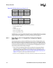
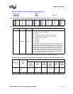
Table 6-26 provides a comparison of supported Asynchronous Static Memory types.
2:0 Read/Write RTx<2:0>
ROM TYPE:
000 – Non-burst ROM or flash Memory
001 – SRAM
010 – Burst-of-four ROM or flash (with non-burst writes)
011 – Burst-of-eight ROM or flash (with non-burst writes)
100 – Variable Latency I/O (VLIO)
101 – Reserved
110 – Reserved
111 – Reserved
Burst refers to the device’s timing. When the subsequent reads from the
device take less time than the first read from a device, it is referred to as
burst timing. The address bits must also be taken into account for burst
timing devices. For example, in a burst-of-four device, only the lower two
non-byte address bits can change for burst timing. For the PXA26x
processor family, this is MA[3:2]. The address order can go 00, 01, 10, 11
where the reads from 01, 10, and 11, take less time to come out of the
device. For burst-of-eight devices, the lower three non-byte address bits
can change. Writes to these devices are non-burst.
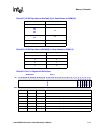
Table 6-25. MSC0/1/2 Register Bit Definitions (Sheet 3 of 3)
0X4800 0008/
0x4800 000C/
0x4800 0010
MSC0/
MSC1/
MSC2
processor
Bit
31 30 29 28 27 26 25 24 23 22 21 20 19 18 17 16 15 14 13 12 11 10 9 8 7 6 5 4 3 2 1 0
RBUFF1/3/5
RRR1/3/5
RDN1/3/5
RDF1/3/5
RBW1/3/5
RT1/3/5
RBUFF0/2/4
RRR0/2/4
RDN0/2/4
RDF0/2/4
RBW0/2/4
RT0/2/4
Reset 0 1 1 1 1 1 1 1 1 1 1 1 0 0 0 0 0 1 1 1 1 1 1 1 1 1 1 1 * 0 0 0
Bits Access Name Description
Table 6-26. Asynchronous Static Memory and Variable Latency I/O Capabilities (Sheet 1 of 2)
MSCx[RTx]
Device
Type
Timing (Memory Clocks)
Burst
Read
Address
Assert
nOE
Assert
Burst
nOE
Deassert
Burst
Write
Address
Assert
nWE
Assert
Burst
nWE
Deassert
000
Non-burst
ROM or
Flash
RDF+1 RDF+1 0 N/A RDF+1 N/A
001 SRAM RDF+1 RDF+1 0 RDN+2 RDN+1 1


