7-28 Intel® PXA26x Processor Family Developer’s Manual
Liquid Crystal Display Controller
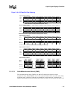
blue pixel components. When CMS=1, monochrome mode is selected, palette entries are 8 bits
wide, 4 or 8 data pins are enabled for single-panel mode, 8 data pins are enabled for dual-panel
mode, and the blue dither block is used.
7.6.1.14 LCD Enable (ENB)
The LCD enable (ENB) bit enables and quickly disables all LCD controller operations. When
ENB=0, the LCD controller is either disabled or in the process of quickly disabling, and all of the
LCD pins can be used for GPIO. When ENB=1, the LCD controller is enabled.
All other control registers must be initialized before setting ENB. LCCR0 can be programmed last,
and all bit fields can be configured at the same time with a word write to the register. If ENB is
cleared while the LCD controller is enabled, the LCD controller immediately stops requesting data
from the LCD DMAC, and the current frame does not complete. The LCD controller must not be
re-enabled until the QD status flag is set in register LCSR, indicating the quick disable is complete.
Quick disable is for sleep shutdown. Regular shutdown of the LCD controller at the end of the
frame can be accomplished via the LCD Disable bit, LCCR0[DIS]. There are separate maskable
interrupts for quick disable and regular disable. See Section 7.2.1, “Enabling the Controller” for
more information.
7.6.2 LCD Controller Control Register 1 (LCCR1)
LCD Controller Control Register 1 contains four bit fields that are used as modulus values for a
collection of down counters, each of which performs a different function to control the timing of
several of the LCD pins. These values must be programmed before enabling the LCD controller.
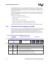
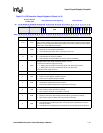
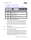
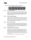
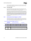
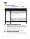
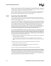
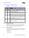
Table 7-4 shows the LCCR1 bit layout. This register may be read or written.
Table 7-4. LCD Controller Control Register 1 (Sheet 1 of 2)
Physical Address
0x4400_0004
LCD Controller Control Register 1 LCD Controller
Bit
31 30 29 28 27 26 25 24 23 22 21 20 19 18 17 16 15 14 13 12 11 10 9 8 7 6 5 4 3 2 1 0
BLW ELW HSW PPL
Reset
0 0 0 0 0 0 0 0 0 0 0 0 0 0 0 0 0 0 0 0 0 0 0 0 0 0 0 0 0 0 0 0
Bits Name Description
31:24 BLW
BEGINNING-OF-LINE PIXEL CLOCK WAIT COUNT (Section 7.6.2.1):
This value (0–255) specifies the number of pixel clock periods to add to the beginning of a
line transmission before the first set of pixels is sent to the display. BOL wait = (BLW + 1).


