


Intel® PXA26x Processor Family Developer’s Manual 6-35
Memory Controller
6.7.1.1 SMROM Memory Options
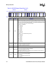
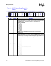
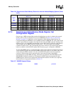
Table 6-16 shows the possible external-to-internal address multiplexing options. For SMROM,
there are no bank-address bits, but the corresponding bits are put on the external address bus. The
number of banks per device always defaults to four.
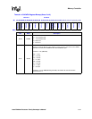
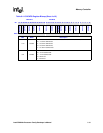
1:0 SXEN0
ENABLE BITS FOR SX MEMORY PARTITION 0 (bit 0) AND PARTITION 1 (bit 1):
0 – Partition is not Enabled as SX Memory
1 – Partition is Enabled as SX Memory
For reset values, see Section 6.11.
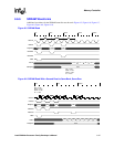
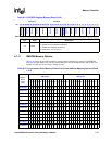
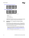
Table 6-14. SXCNFG Register Bitmap (Sheet 6 of 6)
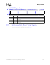
4800 001C SXCNFG
Bit
31 30 29 28 27 26 25 24 23 22 21 20 19 18 17 16 15 14 13 12 11 10 9 8 7 6 5 4 3 2 1 0
Reserved
SXLATCH2
SXTP2
SXCA2
SXRA2
SXRL2
SXCL2
SXEN2
Reserved
SXLATCH0
SXTP0
SXCA0
SXRA0
SXRL0
SXCL0
SXEN0
Reset 0 0 0 0 0 0 0 0 0 0 0 0 0 0 0 0 0 * * * * * * * * * * * * * 0 *
Bits Name Description
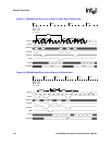
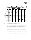
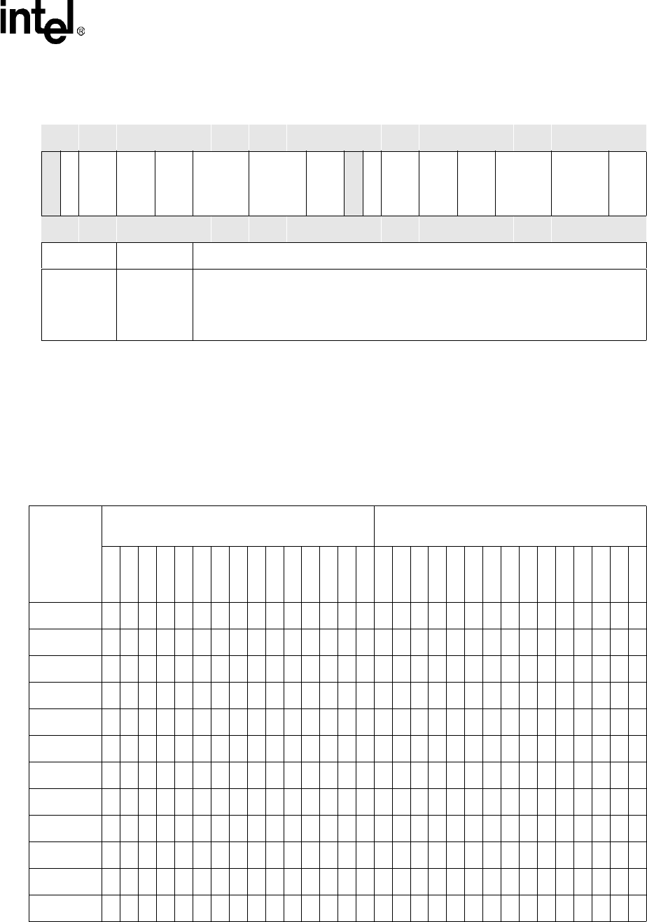
Table 6-16. Synchronous Static Memory External to Internal Address Mapping Options (Sheet
1 of 2)
# Bits
Bank x
Row x
Col x
Data
External Address pins at SXMEM RAS Time
MA<24:10>
External Address pins at SXMEM CAS Time
MA<24:10>
24 23 22 21 20 19 18 17 16 15 14 13 12 11 10 24 23 22 21 20 19 18 17 16 15 14 13 12 11 10
2x12x7x32 222120191817161514131211109 2221 0 8765432
2x12x7x16 21201918171615141312111098 2120 0 7654321
2x12x8x32 2322212019181716151413121110 2322 0 98765432
2x12x8x16 222120191817161514131211109 2221 0 87654321
2x12x9x32 2423222120191817161514131211 2423 0 1098765432
2x12x9x16 2322212019181716151413121110 2322 0 987654321
2x12x10x32 2524232221201918171615141312 2524 0111098765432
2x12x10x16 2423222120191817161514131211 2423 010987654321
2x13x7x32 232221201918171615141312111092322 0 8765432
2x13x7x16 22212019181716151413121110982221 0 7654321
2x13x8x32 2423222120191817161514131211102423 0 98765432
2x13x8x16 232221201918171615141312111092322 0 87654321