


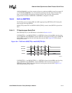
16-12 Intel® PXA26x Processor Family Developer’s Manual
Network/Audio Synchronous Serial Protocol Serial Ports
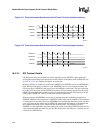
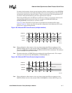
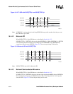
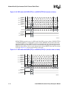
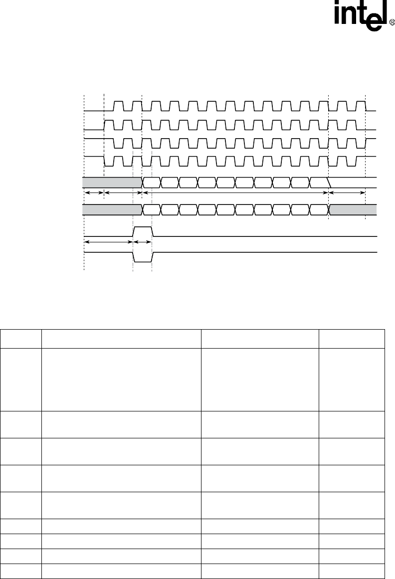
Note: The SSPSFRM delay must not extend beyond the end of T4. SSPSFRM Width must be asserted for
at least 1 SSPSCLK, and must be deasserted before the end of the T4 cycle (i.e. in terms of time,
not bit values, (T5 + T6) <= (T1 + T2 + T3 + T4), 1<= T6 < (T2 + T3 + T4), and (T5 + T6) >= (T1
+ 1) to ensure that SSPSFRM is asserted for at least 2 edges of the SSPSCLK). While the PSP can
be programmed to generate the assertion of SSPSFRM during the middle of the data transfer (after
the MSB was sent), the SSP port is not able to receive data in frame slave mode
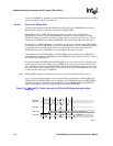
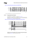
Figure 16-10. Programmable Serial Protocol (single transfers)
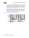
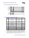
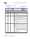
Table 16-2. Programmable Serial Protocol (PSP) Parameters
Symbol Definition Range Units
—
Serial clock mode
(SSPSP[SCMODE])
(Drive, Sample, SSPSCLK Idle)
0 - Fall, Rise, Low
1 - Rise, Fall, Low
2 - Rise, Fall, High
3 - Fall, Rise, High
—
—
Serial frame polarity
(SSPSP[SFRMP])
High or Low —
T1
Start delay
(SSPSP[STRTDLY])
0 - 7 Clock period
T2
Dummy start
(SSPSP[DMYSTRT])
0 - 3 Clock period
T3
Data size
(SSCR0[EDSS] and SSCR0[DSS])
4 - 32 Clock period
T4 Dummy stop (SSPSP[DMYSTOP]) 0 - 3 Clock period
T5 SSPSFRM delay (SSPSP[SFRMDLY] 0 - 88 Half clock period
T6 SSPSFRM width (SSPSP[SFRMWDTH] 1 - 44 Clock period
End of transfer data state (SSPSP[ETDS]) Low or [bit 0] —
A9522-02
MSBUndefined
Undefined Undefined
T1 T2 T3 T4
LSB
MSB LSB
End of Transfer
Data State
T6T5
SSPSCLK
(when SCMODE = 0)
SSPSCLK
(when SCMODE = 1)
SSPSCLK
(when SCMODE = 2)
SSPSCLK
(when SCMODE = 3)
SSPSFRM
(when SFRMP = 1)
SSPSFRM
(when SFRMP = 0)
SSPTXD
SSPRXD