Intel® PXA26x Processor Family Developer’s Manual 11-11
Fast Infrared Communication Port
11.3.3 FICP Control Register 2
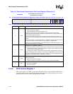
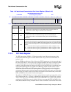
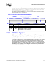
The FICP control register 2 (ICCR2) contains two bit fields that control the polarity of the transmit
and receive data pins and two bits that determine the trigger level for the receive FIFO. The FICP
must be disabled (RXE=TXE=0) when these bits are changed.
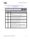
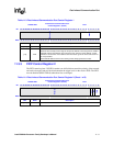
Table 11-3. Fast Infrared Communication Port Control Register 1
0x4080 0004
Fast Infrared Communication Port
Control Register 1 (ICCR1)
FICP
Bit
31 30 29 28 27 26 25 24 23 22 21 20 19 18 17 16 15 14 13 12 11 10 9 8 7 6 5 4 3 2 1 0
Reserved
AMV
Reset 0 0 0 0 0 0 0 0 0 0 0 0 0 0 0 0 0 0 0 0 0 0 0 0 0 0 0 0 0 0 0 0
Bits Name Description
[31:8] — Reserved
[7:0] AMV
ADDRESS MATCH VALUE:
The 8-bit value used by receiver logic to compare to address of incoming frames. If AME=1
and AMV matches the address of the incoming frame, store the frame address, control,
and data in receive FIFO. If the address does not match, ignore the frame and search for
the next preamble.
The broadcast address 0xFF in the incoming frame always generates a match.
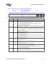
Table 11-4. Fast Infrared Communication Port Control Register 2 (Sheet 1 of 2)
0x4080 0008
Fast Infrared Communication Port
Control Register 2 (ICCR2)
FICP
Bit
31 30 29 28 27 26 25 24 23 22 21 20 19 18 17 16 15 14 13 12 11 10 9 8 7 6 5 4 3 2 1 0
Reserved
RXP
TXP
TRIG
Reset 0 0 0 0 0 0 0 0 0 0 0 0 0 0 0 0 0 0 0 0 0 0 0 0 0 0 0 0 1 1 0 0
Bits Name Description
[31:4] — Reserved


