


Intel® PXA26x Processor Family Developer’s Manual 4-7
System Integration Unit
4.1.3 GPIO Register Definitions
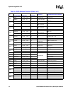
There are a total of twenty-seven 32-bit registers within the GPIO control block. There are nine
distinct register functions and there are three sets of each of the nine registers to serve the 90
GPIOs. The various functions of the nine registers corresponding to each GPIO pin are described
here:
• Three monitor pin state (GPLR)
• Six control output pin state (GPSR, GPCR)
• Three control pin direction (GPDR)
• Six control whether rising edges or falling edges are detected (GRER & GFER)
• Three indicate when specified edge types have been detected on pins (GEDR).
• Six determine whether a pin is used as a normal GPIO or whether it is to be taken over by one
of three possible alternate functions (GAFR_L, GAFR_U).
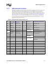
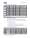
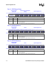
GP86
††
nSDCS[2] ALT_FN_0_OUT 00 Memory Controller SDRAM chip select 2
GPIO Output ALT_FN_1_OUT 01 GPIO
GPIO Input ALT_FN_1_IN 01 GPIO
GP87
††
nSDCS[3] ALT_FN_0_OUT 00 Memory Controller SDRAM chip select 3
GPIO Output ALT_FN_1_OUT 01 GPIO GPIO output
GPIO Input ALT_FN_1_IN 01 GPIO GPIO input
GP88
††
RDnWR ALT_FN_0_OUT 00 Memory Controller Read/write
GPIO Output ALT_FN_1_OUT 01 GPIO GPIO output
GPIO Input ALT_FN_1_IN 01 GPIO GPIO input
GP89
††
nACRESET ALT_FN_0_OUT 00 AC 97 AC 97 reset
GPIO Output ALT_FN_1_OUT 01 GPIO GPIO output
GPIO Input ALT_FN_1_IN 01 GPIO GPIO input
† CKEN[11] - USB Unit Clock Enable bit must be enabled to allow the 48-MHz clock output on GP7
†† GP[89:86] default to their dedicated functionality. To use these pins as GPIOs require selecting ALT_FN_1. Their direction bits
are also reversed from the other GPIOs.
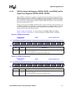
Table 4-1. GPIO Alternate Functions (Sheet 5 of 5)
Pin
Alternate
Function Name
Alternate Function
Assignment
AF{n}
encoding
Source Unit Signal Description and comments
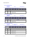
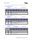
Table 4-2. GPIO Register Definitions (Sheet 1 of 2)
Register
Type
Register Function GPIO[15:0] GPIO[31:16] GPIO[47:32] GPIO[63:48] GPIO[79:64] GPIO[80]
GPLR Monitor Pin State GPLR0 GPLR1 GPLR2
GPSR
Control Output
Pin State
GPSR0 GPSR1 GPSR2
GPCR GPCR0 GPCR1 GPCR2
GPDR Set Pin Direction GPDR0 GPDR1 GPDR2
GRER
Detect Rising/Falling
Edge
GRER0 GRER1 GRER2
GFER GFER0 GFER1 GFER2