Intel® PXA26x Processor Family Developer’s Manual 16-5
Network/Audio Synchronous Serial Protocol Serial Ports
• For PSP, the protocol allows for the configuration of which edge of the SSPSCLK is used for
switching transmit data and the edge for sampling receive data. In addition, the idle state for
SSPSCLK can be controlled and the number of active clocks that precede and follow the data
transmission. Master and slave modes are supported.
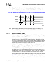
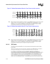
Microwire* uses a half-duplex, master-slave messaging protocol. At the start of a frame, the
controller transmits a one or two-byte control message to the peripheral; no data is sent by the
peripheral. The peripheral interprets the message and if the message is a read request, the
peripheral responds with the requested data, one clock after the last bit of the request message.
Return data—part of the same frame—can be from four to 16-bits in length. The total frame length
is 13 to 33 bits. The SSPSCLK is active during the entire frame.
Note: The serial clock (SSPSCLK), if driven by the SSP port, toggles only while an active data transfer is
underway, unless receive-without-transmit mode is enabled by setting SSCR1[RWOT] and the
frame format is not Microwire*, in which case the SSPSCLK toggles regardless of whether
transmit data exist within the transmit FIFO. At other times, SSPSCLK holds in an inactive or idle
state as defined by the protocol.
16.4.3.1 TI Synchronous Serial Protocol* Details
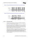
When outgoing data in the SSP port controller is ready to transmit, SSPSFRM asserts for one clock
period. On the following clock, data to be transmitted is driven on SSPTXD one bit at a time, the
most significant bit first. For receive data, the peripheral similarly drives data on the SSPRXD pin.
The word length can be from four to 32-bits. All output transitions occur on the rising edge of
SSPSCLK while data sampling occurs on the falling edge. At the end of the transfer, the SSPTXD
signal either retains the value of the last bit sent (LSB) or clears depending on the serial form and
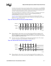
the value of the SSPSP[ETDS] (See Figure 16-1 through Figure 16-8). If the SSP port is disabled
or reset, SSPTXD is forced low.
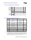
Figure 16-1 shows the TI Synchronous Serial Protocol for when back-to-back frames are
transmitted. Figure 16-2 shows the TI Synchronous Serial Protocol for a single transmitted frame.
Once the transmit FIFO contains data, SSPSFRM is pulsed high for one SSPSCLK period and the
value to be transmitted is transferred from the transmit FIFO to the transmit logic serial shift
register. On the next rising edge of SSPSCLK, the most significant bit of the four to 32-bit data
frame is shifted to the SSPTXD pin. Likewise, the MSB of the received data is shifted onto the
SSPRXD pin by the off-chip serial slave device. Both the SSP and the off-chip serial slave device
then latch each data bit into the serial shifter on the falling edge of each SSPSCLK. The received
data is transferred from the serial shifter to the receive FIFO on the first rising edge of SSPSCLK
after the last bit has been latched.
For back-to-back transfers, the start of one frame is the completion of the previous frame. The
MSB of one transfer immediately follows the LSB of the preceding with no “dead” time between
them. When the SSP port is a master to the frame sync (SSPSFRM) and a slave to the clock
(SSPSCLK), at least three extra clocks are needed at the beginning and end of each block of
transfers to synchronize internal control signals (a block of transfers is a group of back-to-back
continuous transfers).


