Intel® PXA26x Processor Family Developer’s Manual 6-37
Memory Controller
6.7.3 Synchronous Static Memory Timing Diagrams
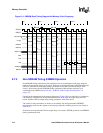
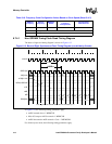
A three-beat read cycle for SMROM is shown in Figure 6-11.
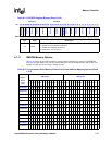
Bit 31 30 29 28 27 26 25 24 23 22 21 20 19 18 17 16 15 14 13 12 11 10 9 8 7 6 5 4 3 2 1 0
Reserved
SXMRS2
Reserved
SXMRS0
Reset 0 0 0 0 0 0 1 0 0 0 1 1 0 0 1 0 0 0 0 0 0 0 1 0 0 0 1 1 0 0 1 0
Bits Name Description
31 — Reserved
30:16 SXMRS2
MRS value to be written to Synchronous Static memory requiring an MRS command for
Bank Pair 2
15 — Reserved
14:0 SXMRS0
MRS value to be written to Synchronous Static Memory requiring an MRS command for
Bank Pair 0
Table 6-17. SXMRS Register Bitmap


