


6-32 Intel® PXA26x Processor Family Developer’s Manual
Memory Controller
20:18 SXCL2
CAS LATENCY FOR SX MEMORY PARTITION PAIR 2/3:
Number of external SDCLK cycles between receiving the READ command and latching the
data. The unit size for SXCL2 is the external SDCLK cycle. When SX Memory runs at half
the memory clock frequency (MDREFR:K0DB2 = 1), the delay is 2*memclk. When in doubt
as to which CAS Latency to use, use the next larger.
IF SXTP2 = 00”(SMROM):
000 – Reserved
001 – Reserved
010 – 3 clocks
011 – 4 clocks
100 – 5 clocks
101 – 6 clocks
110 – Reserved
111 – Reserved
IF SXTP2 = 10 (non-SDRAM timing fast flash)
000 – Reserved
001 – Reserved
010 – 3 clocks
011 – 4 clocks
100 – 5 clocks
101 – 6 clocks
110 – 7 clocks
111 – Reserved
17:16 SXEN2
ENABLE BITS FOR SX MEMORY PARTITION 2 (BIT 16) AND PARTITION 3 (bit 17):
0 – Partition is not Enabled as SX Memory
1 – Partition is Enabled as SX Memory
15 — Reserved
14 SXLATCH0
SXMEM LATCHING SCHEME FOR PAIR 0/1:
0 – Latch return data with fixed delay on MEMCLK
1 – Latch return data with return clock
Must always be written with a 1 to enable the return clock SDCLK for latching data. For
more detail on this return data latching.
13:12 SXTP0
SX MEMORY TYPE FOR PARTITION PAIR 0/1:
00 – Synchronous Mask ROM (SMROM)
01 – Reserved
10 – non-SDRAM-like synchronous flash
11 – Reserved
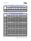
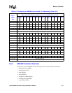
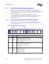
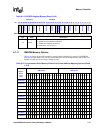
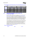
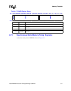
Table 6-14. SXCNFG Register Bitmap (Sheet 3 of 6)
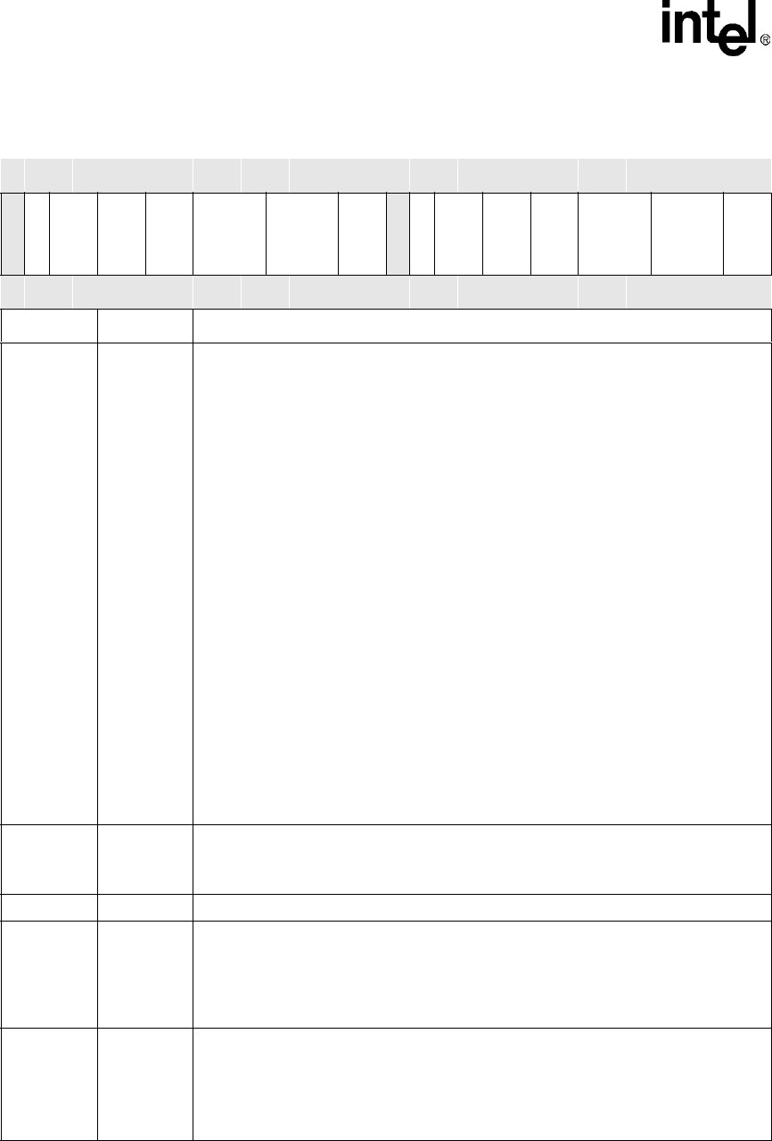
4800 001C SXCNFG
Bit
31 30 29 28 27 26 25 24 23 22 21 20 19 18 17 16 15 14 13 12 11 10 9 8 7 6 5 4 3 2 1 0
Reserved
SXLATCH2
SXTP2
SXCA2
SXRA2
SXRL2
SXCL2
SXEN2
Reserved
SXLATCH0
SXTP0
SXCA0
SXRA0
SXRL0
SXCL0
SXEN0
Reset 0 0 0 0 0 0 0 0 0 0 0 0 0 0 0 0 0 * * * * * * * * * * * * * 0 *
Bits Name Description