10-10 Intel® PXA26x Processor Family Developer’s Manual
Universal Asynchronous Receiver/Transmitter
Note: To ensure that the DMA controller and programmed I/O do not access the same FIFO, software
must not set the DMAE while the TIE or RAVIE bits are set to a 1.
10.4.2.5 Interrupt Identification Register (IIR)
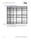
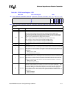
The UART prioritizes interrupts in four levels (see Table 10-8) and records them in the IIR. The
IIR stores information that indicates that a prioritized interrupt is pending and identifies the source
of the interrupt.
In FIFO mode, the received data is available interrupt (priority level 2) takes priority over the
character timeout indication interrupt (priority level 2). For example, if the UART is in FIFO mode
and FIFO Control Register[ITL] = 0b00, this causes the UART to generate an interrupt when there
is one byte in the FIFO. In this scenario, if there is one byte in the FIFO, an interrupt is generated,
and IIR[3:0] = 0b0100, which indicates that received data is available. If data remains in the FIFO
and if a character timeout occurs (no data has been sent for 4 character times), then the interrupt
status does not change to IIR[3:0] = 0b1100 (character timeout indication).
The error interrupt is reported separately in the LSR. In DMA mode, software must check for the
error interrupt before it checks the IIR.
If additional data is received before a character timeout indication interrupt is serviced, the
interrupt is deasserted.
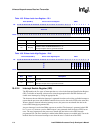
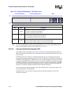
2RLSE
RECEIVER LINE STATUS INTERRUPT ENABLE:
0 – Receiver Line Status interrupt disabled
1 – Receiver Line Status interrupt enabled
1TIE
TRANSMIT DATA REQUEST INTERRUPT ENABLE:
0 – Transmit FIFO Data Request interrupt disabled
1 – Transmit FIFO Data Request interrupt enabled
0RAVIE
RECEIVER DATA AVAILABLE INTERRUPT ENABLE:
0 – Receiver Data Available (Trigger level reached) interrupt disabled
1 – Receiver Data Available (Trigger level reached) interrupt enabled
Table 10-7. Interrupt Enable Register – IER (Sheet 2 of 2)
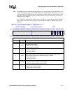
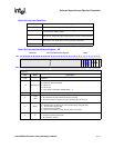
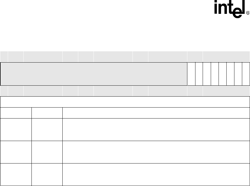
Base+0x04 (DLAB=0) Interrupt Enable Register UART
Bit
31 30 29 28 27 26 25 24 23 22 21 20 19 18 17 16 15 14 13 12 11 10 9 8 7 6 5 4 3 2 1 0
Reserved
DMAE
UUE
NRZE
RTOIE
MIE
RLSE
TIE
RAVIE
Reset 0 0 0 0 0 0 0 0 0 0 0 0 0 0 0 0 0 0 0 0 0 0 0 0 0 0 0 0 0 0 0 0
Read/Write
Bits Name Description


