Intel® PXA26x Processor Family Developer’s Manual 7-35
Liquid Crystal Display Controller
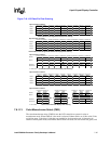
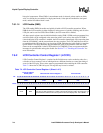
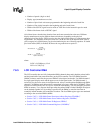
0b100 = 16-bit pixels
0b101–0b111 = reserved
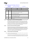
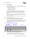
7.6.4.3 Output Enable Polarity (OEP)
In active display mode (LCCR0[PAS]=1), the OEP bit selects the active and inactive states of the
output enable signal (L_BIAS). In this mode, the AC bias pin serves as an enable that signals the
off-chip device when data is actively being driven using the pixel clock, which continuously
toggles in active mode. When OEP=0, L_BIAS is active high and inactive low. When OEP=1,
L_BIAS is active low and inactive high. When L_BIAS is in its active state, data is driven onto the
LCD data pins on the programmed edge of the pixel clock.
In passive display mode, OEP does not affect L_BIAS.
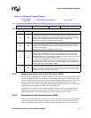
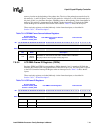
7.6.4.4 Pixel Clock Polarity (PCP)
The PCP bit selects the edge of the pixel clock (L_PCLK) on which data is sampled at the LCD
pins. When PCP=0, sampling occurs on the rising edge of L_PCLK. When PCP=1, sampling
occurs on the falling edge. PCP does not affect the timing of data being driven, it simply inverts
L_PCLK.
7.6.4.5 Horizontal Sync Polarity (HSP)
The HSP bit selects the active and inactive states of the L_LCLK pin. When HSP=0, L_LCLK is
active high and inactive low. When HSP=1, it is active low and inactive high. In active display
mode, L_LCLK serves as the horizontal sync signal and in passive display mode, it is the line
clock.
In both active and passive display modes, the L_FCLK pin is forced to its inactive state whenever
pixels are transmitted. After the end of each line and a programmable number of pixel clocks occur
(controlled by LCCR1[ELW]), the L_FCLK pin is forced to its active state for a programmable
number of line clocks (controlled by LCCR1[HSW]), and is then again forced to its inactive state.
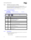
7.6.4.6 Vertical Sync Polarity (VSP)
The VSP bit selects the active and inactive states of the L_FCLK pin. When VSP=0, L_FCLK is
active high and inactive low. When VSP=1, L_FCLK is active low and inactive high.
In active display mode (LCCR0[PAS]=1), L_FCLK serves as the vertical sync signal. It is forced to
its inactive state while pixels are transmitted during the frame. After the end of the frame and a
programmable number of line clocks occur (controlled by LCCR2[EFW]), it is forced to its active
state for a programmable number of line clocks (controlled by LCCR2[VSW]), and is then again
forced to its inactive state.
In passive display mode, L_FCLK serves as the frame clock. It is forced to its active state on the
rising edge of the first pixel clock of each frame. It remains active during the transmission of the
entire first line of pixels in the frame and is then forced back to its inactive state on the rising edge
of the first pixel clock of the second line of the frame. It remains at this state through the end of the
frame.


