


6-8 Intel® PXA26x Processor Family Developer’s Manual
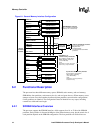
Memory Controller
If memory does not occupy all 64 MB of the partition, reads and writes from or to the unoccupied
portion are processed as if the memory occupies the entire 64 MB of the memory partition.
A single word (or half-word if the data bus width is defined as 16-bits) access to a disabled
SDRAM partition (MDCNFG:DEx=0) causes a CBR refresh cycle to all four partitions. This
technique is used in the hardware initialization procedure. Read return data is indeterminate and
writes are not executed on the external memory bus.
A burst read access to a disabled SDRAM partition results in a target-abort exception. Target aborts
are also generated for burst writes to flash/ROM space and bursts to configuration space.
Attempted single beat writes to ROM are not aborted. Bursts to configuration space also result in
target aborts. Target aborts can be either Data or Prefetch abort depending on the source of the
attempted burst transaction.
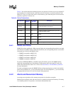
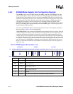
6.5 Memory Configuration Registers
Table 6-2 shows the registers associated with the memory interface and the physical addresses used
to access them. These registers must be mapped as non-cache-able and non-bufferable and can only
be a single word access. They are grouped together in one page and all have the same memory
protections.
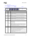
Table 6-2. Memory Interface Control Registers
Physical Address Symbol Register Name
0x4800 0000 MDCNFG SDRAM Configuration Register
0x4800 0004 MDREFR SDRAM Refresh Control Register
0x4800 0008 MSC0 Static Memory Control Register 0
0x4800 000C MSC1 Static Memory Control Register 1
0x4800 0010 MSC2 Static Memory Control Register 2
0x4800 0014 MECR
Expansion Memory (16-bit PC Card / Compact Flash) Bus
Configuration Register
0x4800 001C SXCNFG Synchronous Static Memory Control Register
0x4800 0024 SXMRS MRS value to be written to SMROM
0x4800 0028 MCMEM0
Card interface Common Memory Space Socket 0 Timing
Configuration
0x4800 002C MCMEM1
Card interface Common Memory Space Socket 1 Timing
Configuration
0x4800 0030 MCATT0 Card interface Attribute Space Socket 0 Timing Configuration
0x4800 0034 MCATT1 Card interface Attribute Space Socket 1 Timing Configuration
0x4800 0038 MCIO0 Card interface I/O Space Socket 0 Timing Configuration
0x4800 003C MCIO1 Card interface I/O Space Socket 1 Timing Configuration
0x4800 0040 MDMRS MRS value to be written to SDRAM
0x4800 0044 BOOT_DEF
Read-Only Boot-time register. Contains BOOT_SEL and
PKG_SEL values.
0x4800 0058 MDMRSLP
Low-Power SDRAM Mode Register Set Configuration
Register
0x4800 0064 SA1111CR SA1111 compatibility register