


6-16 Intel® PXA26x Processor Family Developer’s Manual
Memory Controller
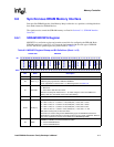
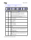
19 K2DB2
SDRAM CLOCK PIN 2 (SDCLK2) DIVIDE BY 2 CONTROL/STATUS:
0 – SDCLK2 is same frequency as MEMCLK
1 – SDCLK2 runs at one-half the MEMCLK frequency
18 K2RUN
SDRAM CLOCK PIN 2 (SDCLK<2>) RUN CONTROL/STATUS:
0 – SDCLK2 disabled
1 – SDCLK2 enabled
K2RUN also can be cleared by program. Use with caution because the resulting state
prohibits automatic transitions for any commands.
Setting K1RUN or K2RUN is a part of the hardware and sleep reset procedure for SDRAM.
17 K1DB2
SDRAM CLOCK PIN 1 (SDCLK1) DIVIDE BY 2 CONTROL/STATUS:
0 – SDCLK1 is same frequency as MEMCLK
1 – SDCLK1 runs at one-half the MEMCLK frequency
16 K1RUN
SDRAM CLOCK PIN 1 (SDCLK<1>) RUN CONTROL/STATUS:
0 – SDCLK1 disabled
1 – SDCLK1 enabled
K1RUN can be cleared by software. Use with caution because the resulting state prohibits
automatic transitions for any commands.
Setting K1RUN or K2RUN is a part of the hardware and sleep reset procedure for SDRAM.
15 E1PIN
SDRAM CLOCK ENABLE PIN 1 (SDCKE1) LEVEL CONTROL/STATUS:
0 – SDCKE1 is disabled
1 – SDCKE1 is enabled
E1PIN can be cleared by program to cause a power-down command (if K1RUN=1 or
K2RUN=1, and SLFRSH=0). Use with caution because the resulting state prohibits
automatic transitions for mode register set, read, write, and refresh commands. E1PIN can
be set by program to cause a power-down-exit command (if K1RUN=1 or K2RUN=1, and
SLFRSH=0).
Setting E1PIN is a part of the hardware reset or sleep reset procedure for SDRAM.
14 K0DB2
SYNCHRONOUS STATIC MEMORY CLOCK PIN 0 (SDCLK<0>) DIVIDE BY 2
CONTROL/STATUS:
0 – SDCLK0 runs at the memory clock frequency.
1 – SDCLK0 runs at one-half the memory clock frequency.
This bit is automatically set upon hardware or sleep reset.
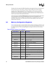
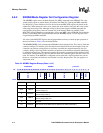
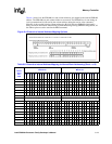
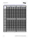
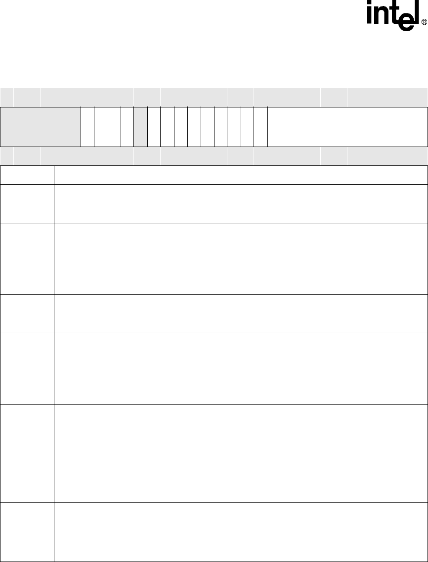
Table 6-6. MDREFR Register Bitmap (Sheet 2 of 3)
4800 0004 MDREFR processor
Bit
31 30 29 28 27 26 25 24 23 22 21 20 19 18 17 16 15 14 13 12 11 10 9 8 7 6 5 4 3 2 1 0
Reserved
K2FREE
K1FREE
K0FREE
SLFRSH
Reserved
APD
K2DB2
K2RUN
K1DB2
K1RUN
E1PIN
K0DB2
K0RUN
E0PIN
DRI
Reset 0 0 0 0 0 0 1 1 1 1 0 0 1 0 1 0 0 1 * * 1 1 1 1 1 1 1 1 1 1 1 1
Bits Name Description