


17-10 Intel® PXA26x Processor Family Developer’s Manual
Hardware UART
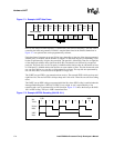
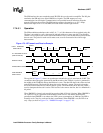
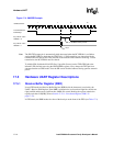
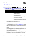
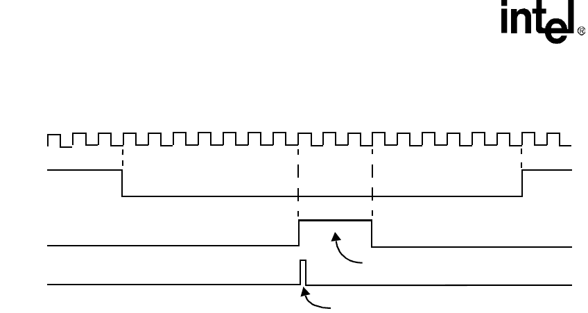
Figure 17-4. XMODE Example.
Note: The SIR TXD output pin is automatically held deasserted when the RCVEIR bit is set. Before
setting the RCVEIR bit, check that the TEMT bit is 1. While receiving, any data placed in the
transmit FIFO will not be held. Only add data to the transmit FIFO while not receiving. To start
transmission, the RCVEIR bit must be cleared.
To disable SIR, disable the IrDA LED first, if possible. Second, set the TXD GPIO pin to the
infrared LED's default state using the GPCR/GPSR registers. Next, change the TXD pin from
alternate function to GPIO mode. Now the SIR can be disabled without causing spurious transmit
pulses.
17.5 Hardware UART Register Descriptions
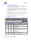
17.5.1 Receive Buffer Register (RBR)
In non-FIFO mode, the Receive Buffer Register (RBR) holds the character(s) received by the
UART’s Receive Shift Register. If the RBR is configured to use fewer than eight bits, the bits are
right-justified and the most significant bits (MSB) are zeroed. Reading the register empties the
register and clears LSR[DR]
(refer to Section 17.5.11, “Line Status Register (LSR)” on
page 17-23
).
In FIFO mode, the RBR latches the value of the data byte at the front of the FIFO
(see Table 17-2).
1
7
11 16
1.6 µs
3 16X BAUD Clock periods
IR_TXD Pin value
XMODE = 1
IR_TXD Pin value
XMODE = 0
Transmit Start bit
followed by 1
16X Baud Clock