Intel® PXA26x Processor Family Developer’s Manual 10-15
Universal Asynchronous Receiver/Transmitter
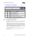
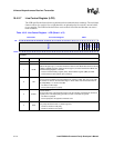
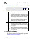
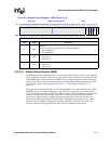
10.4.2.8 Line Status Register (LSR)
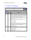
The LSR provides data transfer status information to the processor.
In non-FIFO mode, LSR[4:2]: parity error, framing error, and break interrupt, show the error status
of the character that has just been received.
In FIFO mode, LSR[4:2] show the status bits of the character that is currently at the front of the
FIFO.
LSR[4:1] produce a receiver line status interrupt when the corresponding conditions are detected
and the interrupt is enabled. In FIFO mode, the receiver line status interrupt only occurs when the
erroneous character reaches the front of the FIFO. If the erroneous character is not at the front of
the FIFO, a line status interrupt is generated after the other characters are read and the erroneous
character becomes the character at the front of the FIFO.
The LSR must be read before the erroneous character is read. LSR[4:1] bits are set until software
reads the LSR.
See Section 10.4.5, “DMA Requests” for details on using the DMA to receive data.
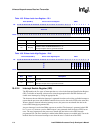
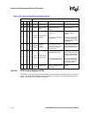
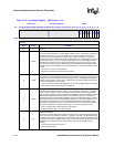
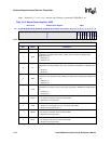
3PEN
PARITY ENABLE:
Enables a parity bit to be generated on transmission or checked on reception.
0 – No parity
1 – Parity
2STB
STOP BITS:
Specifies the number of stop bits transmitted and received in each character. When
receiving, the receiver only checks the first stop bit.
0 – 1 stop bit
1 – 2 stop bits, except for 5-bit character then 1-1/2 bits
1:0 WLS[1:0]
WORD LENGTH SELECT:
Specifies the number of data bits in each transmitted or received character.
00 – 5-bit character
01 – 6-bit character
10 – 7-bit character
11 – 8-bit character
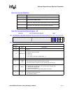
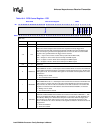
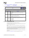
Table 10-12. Line Control Register – LCR (Sheet 2 of 2)
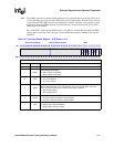
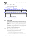
Base+0x0C Line Control Register UART
Bit
31 30 29 28 27 26 25 24 23 22 21 20 19 18 17 16 15 14 13 12 11 10 9 8 7 6 5 4 3 2 1 0
Reserved
DLAB
SB
STKYP
EPS
PEN
STB
WLS1
WLS0
Reset 0 0 0 0 0 0 0 0 0 0 0 0 0 0 0 0 0 0 0 0 0 0 0 0 0 0 0 0 0 0 0 0
Read/Write
Bits Name Description


