


5-20 Intel® PXA26x Processor Family Developer’s Manual
Direct Memory Access Controller
5.3.4 DMA Descriptor Address Registers
The DMA Descriptor Address Registers (DDADRx) (see Table 5-9, “DMA Descriptor Address
Register Bit Definitions” on page 5-21) contain the memory address of the next descriptor for a
specific channel. On power up, the bits in this register are undefined. The address must be aligned
to a 16-byte boundary. This means that bits [3:1] of the address are reserved and must be read and
written as zeroes. DDADR must not contain the address of any other internal peripheral register or
DMA register.
DDADR is reserved if the channel is no-descriptor fetch mode.
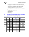
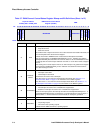
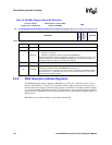
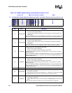
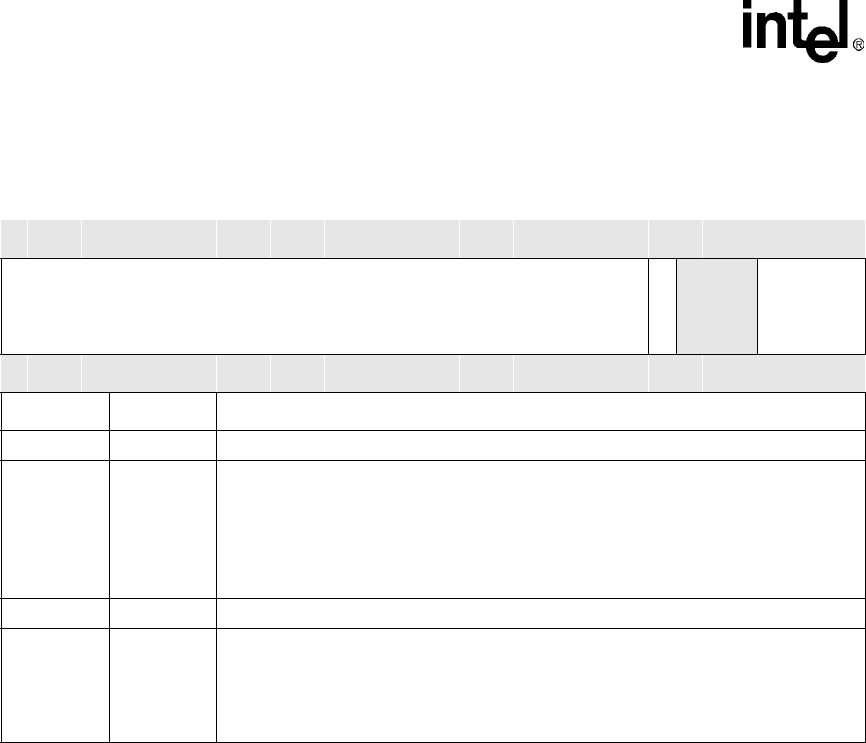
Table 5-8. DRCMRx Registers Bitmap Bit Definitions
Physical Address
0x4000_0100 - 0x4000_019C
DMA Request to Channel Map
Register (DRCMRx)
DMA
Bit
31 30 29 28 27 26 25 24 23 22 21 20 19 18 17 16 15 14 13 12 11 10 9 8 7 6 5 4 3 2 1 0
RESERVED
MAPVLD
RESERVED
CHLNUM
Reset
0 0 0 0 0 0 0 0 0 0 0 0 0 0 0 0 0 0 0 0 0 0 0 0 0 0 0 0 0 0 0 0
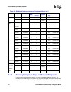
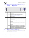
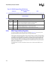
Bits Name Description
31:8 — Reserved – Read as unknown and must be written as zero.
7 MAPVLD
MAP VALID (read / write):
0 – Request is unmapped
1 – Request is mapped to a channel indicated by DRCMRx[3:0]
Determines whether the request is mapped to a channel or not. If the bit is set to a 1, the
request is mapped to a channel indicated in DRCMRx[3:0]. If the bit is 0, the request is
unmapped. This bit can also be used to mask the request.
6:4 — Reserved – Read as unknown and must be written as zero.
3:0 CHLNUM
CHANNEL NUMBER (read / write):
Indicates the channel number if DRCMR[MAPVLD] is set to a 1.
Do not map two active requests to the same channel. It produces unpredictable results.
Refer to Section 5.1.3, “Direct Memory Access Channel Priority Scheme” on page 5-4 to
review the channel priority scheme.