Intel® PXA26x Processor Family Developer’s Manual 3-3
Clocks and Power Manager
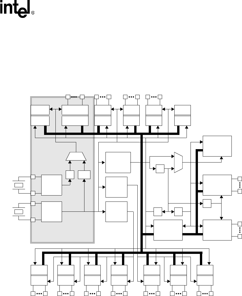
Figure 3-1 shows a functional representation of the clocking network. “L” is in the core PLL.
The PXbus is the internal bus between the core, the DMA/bridge, the LCD controller, and the
memory controller as shown in Figure 3-1. This bus is clocked at 1/2 the run mode frequency. For
optimal performance, the PXbus should be clocked as fast as possible. For example, if a target core
frequency of 200 MHz is desired use 200-MHz run mode instead of 200-MHz turbo mode with run
at 100 MHz. Increasing the PXbus frequency may help reduce the latency involved in accessing
non-cacheable memory.
Figure 3-1. Clocks Manager Block Diagram
/N
/M
/4
DMA
/
Bridge
/1 /112
UARTs
14.746
AC97
12.288
I2S
5.672
PWM
3.6864
SSP
3.6864
GPIO
3.6864
OST
3.6864
PWR_MGR
32.768 k
32.768
KHz
OSC
3.6864
MHz
OSC
100-400
MHz
PLL*
95.846
MHz
PLL
147.46
MHz
PLL
CORE
CPU
Controller
MEM
Controller
LCD
/2
MMC
19.169
I2C
31.949
FICP
47.923
USB
47.923
RTC
32.768 k
RETAINS POWER IN SLEEP
* For the PXA26x processor family: 100-400 MHz.
PXbus


