Intel® PXA26x Processor Family Developer’s Manual 14-9
Inter-Integrated Circuit Sound Controller
NOTES:
† If ENB is toggled in the middle of a normal operation, the RST bit must also be set and cleared to reset all
I2SC registers.
†† The SACR0[ENB] control signal crosses clock domains. It is registered in an internal clock domain that is
much faster than the BITCLK domain. It takes four BITCLK cycles and four internal clock cycles before
SACR0[ENB] is conveyed to the slower BITCLK domain. If the control setting is modified at a rate faster than
(4 BITCLK + 4 internal clock) cycles, the last updated value in this time frame is stored in a temporary register
and is transferred to the BITCLK domain.
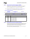
14.6.1.1 Special purpose FIFO Read/Write function
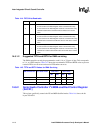
As shown in Table 14-4, EFWR and STRF can be programmed for special purpose FIFO accesses.
Under normal operating conditions, the processor or the DMA controller can only write to the
transmit FIFO and only read the receive FIFO. Programming these bits allows the processor or the
DMA controller to read and write both FIFOs.
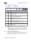
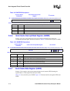
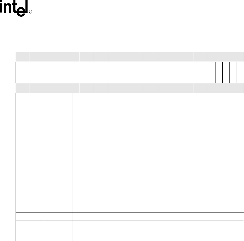
7:6 — Reserved
5STRF
Select transmit or receive FIFO for EFWR based special purpose function:
0 – Transmit FIFO is selected
1 – Receive FIFO is selected
See Table 14-4 for details.
4EFWR
This bit enables a special purpose FIFO Write/Read function:
0 – Special purpose FIFO write/read function is disabled
1 – Special purpose FIFO write/read function is enabled
See Table 14-4 for details.
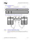
3RST
†
RESET:
Resets FIFOs logic and all registers, except this register (SACR0):
0 – Not reset
1 – Reset is Active to Other Registers
2BCKD
This bit specifies input/output direction of BITCLK:
0 – Input. BITCLK driven by an external source.
1 – Output. BITCLK generated internally and driven out to the CODEC.
1—Reserved
0ENB
† ††
ENABLE I
2
S FUNCTION:
0 – I
2
SLINK is disabled
1 – I
2
SLINK is enabled
Table 14-3. SACR0 Bit Descriptions (Sheet 2 of 2)
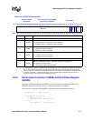
Physical Address
0x4040-0000
Serial Audio Controller Global
Control Register
I
2
S Controller
Bit
31 30 29 28 27 26 25 24 23 22 21 20 19 18 17 16 15 14 13 12 11 10 9 8 7 6 5 4 3 2 1 0
Reserved RFTH TFTH
Reserved
STRF
EFWR
RST
BCKD
Reserved
ENB
Reset 0 0 0 0 0 0 0 0 0 0 0 0 0 0 0 0 0 1 1 1 0 1 1 1 0 0 0 0 0 0 0 0
Bits Name Description


