


17-22 Intel® PXA26x Processor Family Developer’s Manual
Hardware UART
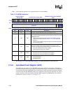
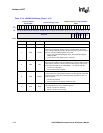
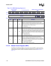
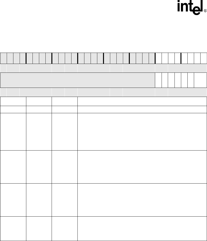
Table 17-14. LCR Bit Definitions (Sheet 1 of 2)
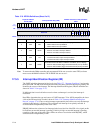
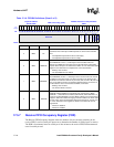
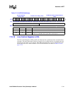
Physical Address
0x4160_000C
Line Control Reg. (LCR)
PXA26x Processor Family Hardware
UART
User
Settings
Bit 31 30 29 28 27 26 25 24 23 22 21 20 19 18 17 16 15 14 13 12 11 10 9 8 7 6 5 4 3 2 1 0
Reserved
DLAB
SB
STKYP
EPS
PEN
STB
WLS
Reset ? ? ? ? ? ? ? ? ? ? ? ? ? ? ? ? ? ? ? ? ? ? ? ? 0 0 0 0 0 0 0 0
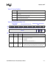
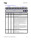
Bits Access Name Description
31:8 N/A — Reserved – Read as unknown and must be written as zero.
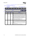
7R/WDLAB
DIVISOR LATCH ACCESS BIT:
Must be set to access the Divisor Latches of the Baud Rate Generator
during a READ or WRITE operation. Must be cleared to access the receiver
buffer, the Transmit Holding Register, or the IER.
0 – access Transmit Holding Register (THR), Receive Buffer Register
(RBR) and IER.
1 – access Divisor Latch registers (DLL and DLH)
6R/WSB
SET BREAK:
Causes a break condition to be transmitted to the receiving UART. Acts only
on the TXD pin and has no effect on the transmitter logic. In FIFO mode,
wait until the transmitter is idle, LSR[TEMT] = 1, to set and clear SB.
0 – no effect on TXD output
1 – forces TXD output to 0 (space)
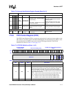
5 R/W STKYP
STICKY PARITY:
Forces the bit value at the parity bit location to be the opposite of the EPS
bit, rather than the parity value. This stops parity generation. If PEN = 0,
STKYP is ignored.
0 – No effect on parity bit
1 – Forces parity bit to be opposite of EPS bit value
4R/WEPS
EVEN PARITY SELECT:
Even parity select bit. If PEN = 0, EPS is ignored.
0 – Sends or checks for odd parity
1 – Sends or checks for even parity