Control of On-Chip Peripherals
8-3
On-Chip Peripherals
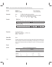
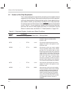
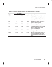
Table 8–1. Peripheral Register Locations and Reset Conditions (Continued)
Register
Name
I/O Address
Register
Name
Effects at ResetReset ValueOther ’C2xx’C209
IOSR – FFF6h 18xxh
I/O status register.
Auto-baud alignment is
disabled. Error and status flags are reset.
The lower eight bits are dependent on the
values on pins IO0, IO1, IO2, and IO3 at
reset.
BRD – FFF7h 0001h
Baud rate divisor register.
A baud rate of
(CLKOUT1 rate)/16 is selected.
TCR FFFCh FFF8h 0000h
Timer control register.
The divide-down
value is 0, and the timer is started.
PRD FFFDh FFF9h FFFFh
Timer period register.
The next value to be
loaded into the timer counter register
(TIM) is at its highest value.
TIM FFFEh FFFAh FFFFh
Timer counter register.
The timer count is
at its highest value.
WSGR
FFFFh FFFCh 0FFFh
Wait-state generator control register.
The
maximum number of wait states are se-
lected for off-chip program, data, and I/O
spaces.


