


Emulation Design Considerations
E-25
Design Considerations for Using XDS510 Emulator
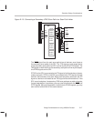
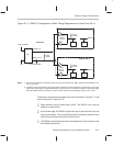
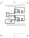
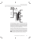
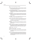
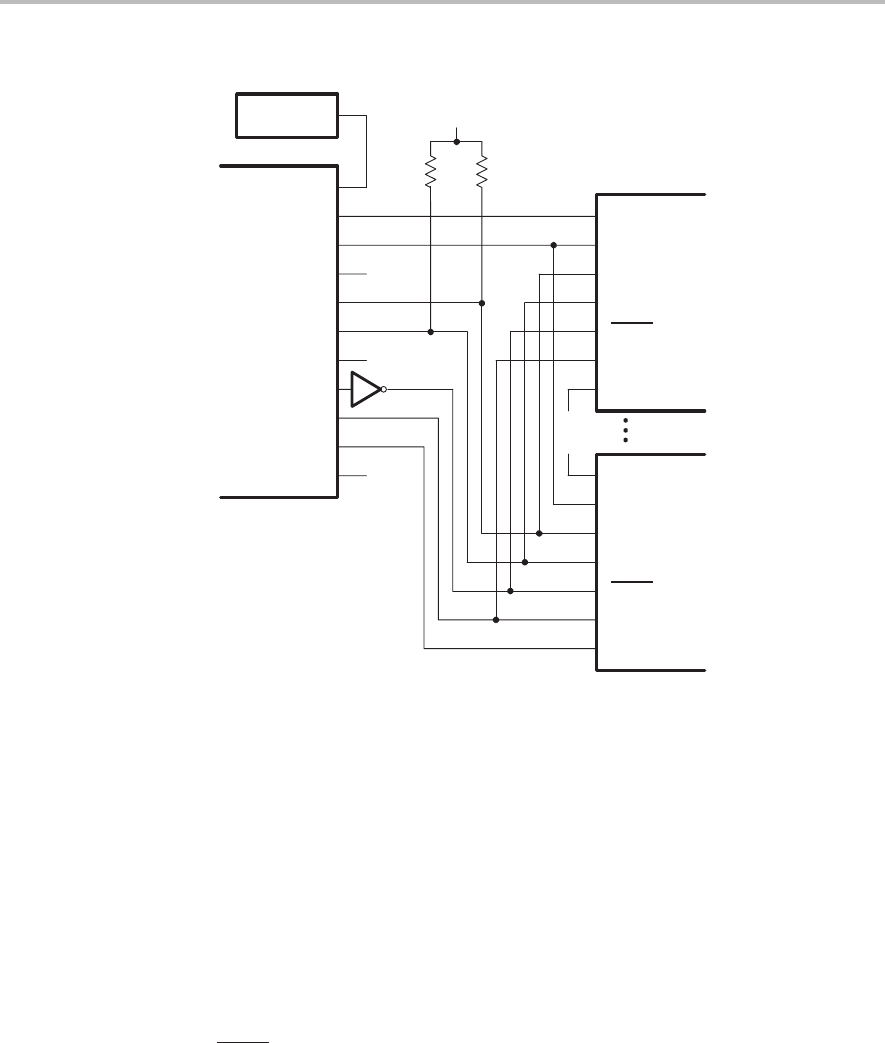
Figure E–15. TBC Emulation Connections for n JTAG Scan Paths
JTAG0
JTAGN
TDI
EMU1
TMS
TDO
EMU0
TRST
TCK
TDO
TCK
TRST
EMU1
EMU0
TMS
TDI
Clock
TDI1
TDI0
TCKO
TMS5/EVNT3
TMS4/EVNT2
TMS3/EVNT1
TMS2/EVNT0
TMS1
TMS0
TDO
TCKI
V
CC
TBC
In the system design shown in Figure E–15, the TBC emulation signals TCKI,
TDO, TMS0, TMS2/EVNT0, TMS3/EVNT1, TMS5/EVNT3, TCKO, and TDI0
are used, and TMS1, TMS4/EVNT2, and TDI1 are not connected. The target
devices’ EMU0 and EMU1 signals are connected to V
CC
through pullup resis-
tors and tied to the TBC’s TMS2/EVNT0 and TMS3/EVNT1 pins, respectively.
The TBC’s TCKI pin is connected to a clock generator. The TCK signal for the
main JTAG scan path is driven by the TBC’s TCKO pin.
On the TBC, the TMS0 pin drives the TMS pins on each device on the main
JTAG scan path. TDO on the TBC connects to TDI on the first device on the
main JTAG scan path. TDI0 on the TBC is connected to the TDO signal of the
last device on the main JTAG scan path. Within the main JTAG scan path, the
TDI signal of a device is connected to the TDO signal of the device before it.
TRST
for the devices can be generated either by inverting the TBC’s
TMS5/EVNT3 signal for software control or by logic on the board itself.