Timer
8-9
On-Chip Peripherals
The TINT request automatically sets the TINT flag bit in the interrupt flag regis-
ter (IFR). You can mask or unmask the request with the interrupt mask register
(IMR). If you are not using the timer, mask TINT so that it does not cause an
unexpected interrupt.
8.4.1 Timer Operation
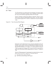
Here is a typical sequence of events for the timer:
1) The PSC decrements on each succeeding CLKOUT1 pulse until it
reaches 0.
2) On the next CLKOUT1 cycle, the TDDR loads the new divide-down count
into the PSC, and the TIM decrements by 1.
3) The PSC and the TIM continue to decrement in the same way until the TIM
decrements to 0.
4) On the next CLKOUT1 cycle, a timer interrupt (TINT) is sent to the CPU,
a pulse is sent to the TOUT pin, the new timer count is loaded from the
PRD into the TIM, and the PSC is decremented once.
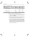
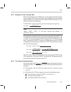
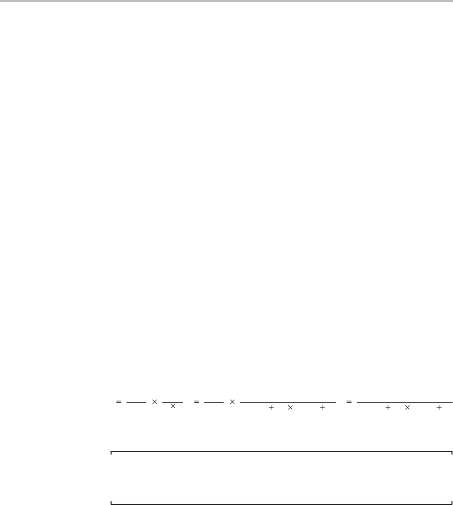
The TIM decrements by one every (TDDR+1) CLKOUT1 cycles. When PRD,
TDDR, or both are nonzero, the timer interrupt rate is defined by Equation 8–1,
where t
c(CO)
is the period of CLKOUT1, u is the TDDR value plus 1, and v is
the PRD value plus 1. When PRD = TDDR = 0, the timer interrupt rate is
(CLKOUT1 rate)/2.
Equation 8–1. Timer Interrupt Rate for Nonzero TDDR and/or PRD
TINT rate
1
t
c(CO)
1
u v
1
t
c(CO)
1
(TDDR 1) (PRD 1)
CLKOUT1 rate
(TDDR 1) (PRD 1)
Note:
Equation 8–1 is not valid for TDDR = PRD = 0; in this case, the timer interrupt
rate defaults to (CLKOUT1 rate)/2.
In Equation 8–1 the timer interrupt rate equals the CLKOUT1 frequency
(1/t
c(CO)
) divided by two independent factors (u and v). Each of the two divisors
is implemented with a down counter and a period register. See the timer func-
tional block diagram, Figure 8–4, on page 8-8. The counter and period regis-
ters for the divisor u are the PSC and TDDR, respectively, both 4-bit fields of
the timer control register (TCR). The counter and period registers for the divi-


