Wait-State Generator
8-15
On-Chip Peripherals
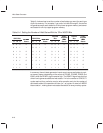
state generator, see subsection 11.4.3 on page 11-16. To avoid bus conflicts,
all writes to external addresses take at least two cycles.
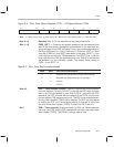
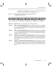
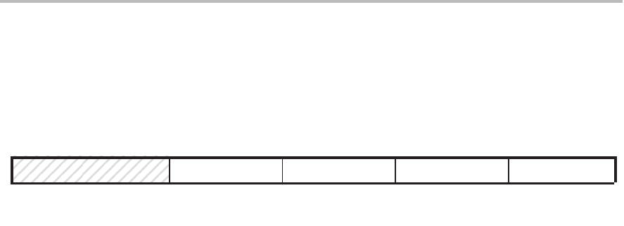
Figure 8–6. ’C2xx Wait-State Generator Control Register (WSGR)
— I/O-Space Address FFFCh
15 14 13 12 11 10 9 8 7 6 5 4 3 2 1 0
Reserved ISWS DSWS PSUWS PSLWS
0 R/W–111 R/W–111 R/W–111 R/W–111
Note: 0 = Always read as zeros; R = Read access; W = Write access; value following dash (–) is value after reset.
Bits 15–12 Reserved. Bits 15–12 are reserved and are always read as 0s.
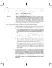
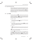
Bits 11–9 ISWS — I/O-space wait-state bits. Bits 9–11 determine the number of wait states
(0, 1, 2, 3, 4, 5, 6, or 7) that are applied to reads from and writes to off-chip I/O space.
At reset, the three ISWS bits become 111, setting seven wait states for reads from and
writes to off-chip I/O space.
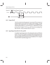
Bits 8–6 DSWS — Data-space wait-state bits. Bits 6–8 determine the number of wait states
(0, 1, 2, 3, 4, 5, 6, or 7) that are applied to reads from and writes to off-chip data space.
At reset, the three DSWS bits become 111, setting seven wait states for reads from
and writes to off-chip data space.
Bits 5–3 PSUWS — Upper program-space wait-state bits. Bits 3–5 determine the number
of wait states (0, 1, 2, 3, 4, 5, 6, or 7) that are applied to reads from and writes to off-
chip
upper
program addresses 8000h–FFFFh. At reset, the three PSUWS bits be-
come 111, setting seven wait states for reads from and writes to off-chip upper pro-
gram space.
Bits 2–0 PSLWS — Lower program-space wait-state bits. Bits 0–2 determine the number
of wait states (0, 1, 2, 3, 4, 5, 6, or 7) that are applied to reads from and writes to off-
chip
lower
program addresses 0h–7FFFh. At reset, the three PSLWS bits become
111, setting seven wait states for reads from and writes to off-chip lower program
space.


